ADF7023-J View Datasheet(PDF) - Analog Devices
Part Name
Description
Manufacturer
ADF7023-J Datasheet PDF : 100 Pages
| |||
ADF7023-J
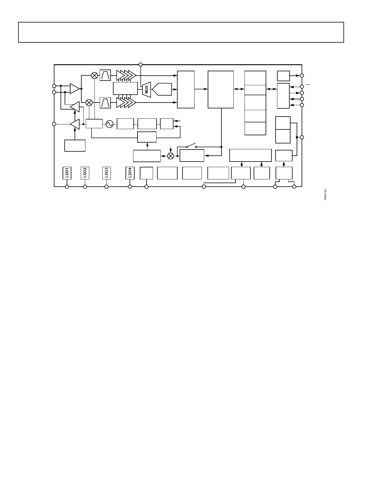
FUNCTIONAL BLOCK DIAGRAM
ADCIN_ATB3
RFIO_1P
RFIO_1N
RFO2
LNA
PA
RSSI/
LOGAMP
8-BIT
ADC
FSK
ASK
DEMOD
CDR
AFC
AGC
PA DIVIDER
LOOP CHARGE
FILTER
PUMP
PFD
26MHz OSC
PA RAMP
PROFILE
ADF7023-J
DIVIDER
Σ-∆
MODULATOR
fDEV
GAUSSIAN
FILTER
8-BIT RISC
PROCESSOR
4kB ROM
MAC
2kB RAM
256 BYTE
PACKET
RAM
64 BYTE
BBRAM
256 BYTE
MCR RAM
WAKE-UP CONTROL
TIMER UNIT
IRQ
CTRL
SPI
GPIO
TEST
DAC
CLOCK
DIVIDER
BIAS
ANALOG
TEST
TEMP
SENSOR
BATTERY
MONITOR
32kHz
OSC
32kHz
RCOSC
26MHz
OSC
IRQ_GP3
CS
MISO
SCLK
MOSI
GPIO1
CREGRFx CREGVCO CREGSYNTH CREGDIGx RBIAS
1GPIO REFERS TO PINS 17, 18, 19, 20, 25, AND 27.
XOSC32KN_ATB2 XOSC32KP_GP5_ATB1 XOSC26N XOSC26P
Figure 1.
GENERAL DESCRIPTION
The ADF7023-J is a very low power, high performance, highly
integrated 2FSK/GFSK/MSK/GMSK transceiver designed for
operation in the 902 MHz to 958 MHz frequency band, which
covers the ARIB Standard T96 band at 950 MHz. Data rates
from 1 kbps to 300 kbps are supported.
The transmit RF synthesizer contains a VCO and a low noise
fractional-N phase locked loop (PLL) with an output channel
frequency resolution of 400 Hz. The VCO operates at twice the
fundamental frequency to reduce spurious emissions. The receive
and transmit synthesizer bandwidths are automatically, and
independently, configured to achieve optimum phase noise,
modulation quality, and settling time. The transmitter output
power is programmable from −20 dBm to +13.5 dBm, with
automatic PA ramping to meet transient spurious specifications.
The part possesses both single-ended and differential PAs, which
allow for Tx antenna diversity.
The receiver is exceptionally linear, achieving an IP3 specification
of −12.2 dBm and −11.5 dBm at maximum gain and minimum
gain, respectively, and an IP2 specification of 18.5 dBm and 27 dBm
at maximum gain and minimum gain, respectively. The receiver
achieves an interference blocking specification of 66 dB at a
±2 MHz offset and 74 dB at a ±10 MHz offset. Thus, the part
is extremely resilient to the presence of interferers in spectrally
noisy environments. The receiver features a novel, high speed,
AFC loop, allowing the PLL to find and correct any RF frequency
errors in the recovered packet. A patent pending image rejection
calibration scheme is available by downloading the image rejection
calibration firmware module to program RAM. The algorithm
does not require the use of an external RF source nor does it
require any user intervention once initiated. The results of the
calibration can be stored in nonvolatile memory for use on
subsequent power-ups of the transceiver.
The ADF7023-J operates with a power supply range of 2.2 V to
3.6 V and has very low power consumption in both Tx and Rx
modes, enabling long lifetimes in battery-operated systems while
maintaining excellent RF performance. The device can enter a
low power sleep mode in which the configuration settings are
retained in the battery backup random access memory (BBRAM).
The ADF7023-J features an ultralow power, on-chip,
communications processor. The communications processor,
which is an 8-bit RISC processor, performs the radio control,
packet management, and smart wake mode (SWM) functionality.
The communications processor eases the processing burden of
the companion processor by integrating the lower layers of a
typical communication protocol stack. The communications
processor also permits the download and execution of firmware
modules. Available modules include image rejection (IR)
calibration, advanced encryption standard (AES) encryption,
and Reed-Solomon coding. These firmware modules are included
in the Applications Software, which is available online at
ftp://ftp.analog.com/pub/RFL/ADF7023/.
The communications processor provides a simple command-based
radio control interface for the host processor. A single-byte command
transitions the radio between states or performs a radio function.
The communications processor provides support for generic
packet formats. The packet format is highly flexible and fully
programmable, thereby ensuring its compatibility with proprietary
packet profiles. In transmit mode, the communications processor
can be configured to add preamble, sync word, and CRC to the
Rev. 0 | Page 4 of 100
Share Link: 