ADG1401BRMZ-REEL7 View Datasheet(PDF) - Analog Devices
Part Name
Description
Manufacturer
ADG1401BRMZ-REEL7 Datasheet PDF : 16 Pages
| |||
ADG1401/ADG1402
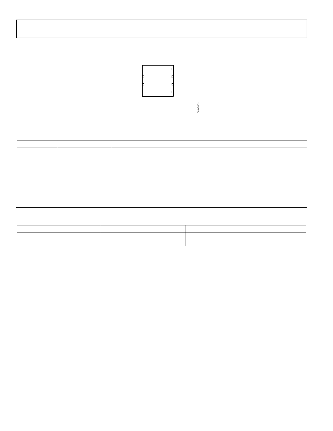
PIN CONFIGURATION AND FUNCTION DESCRIPTIONS
S1
NC 2
GND 3
VDD 4
ADG1401/
ADG1402
TOP VIEW
(Not to Scale)
8D
7 VSS
6 IN
5 NC
NOTES
1. EXPOSED PAD TIED TO SUBSTRATE, VSS.
2. NC = NO CONNECT.
Figure 3. ADG1401/ADG1402 Pin Configuration
Table 7. ADG1401/ADG1402 Pin Function Descriptions
Pin No.
Mnemonic
Description
1
S
Source Terminal. This pin can be an input or output.
2
NC
No Connect.
3
GND
Ground (0 V) Reference.
4
VDD
Most Positive Power Supply Potential.
5
NC
No Connect.
6
IN
Logic Control Input.
7
VSS
Most Negative Power Supply Potential.
8
D
Drain Terminal. This pin can be an input or output.
EPAD
Exposed pad tied to substrate, VSS, for LFCSP package.
Table 8. ADG1401/ADG1402 Truth Table
ADG1401 IN
ADG1402 IN
1
0
0
1
Switch Condition
On
Off
Rev. 0 | Page 8 of 16
Share Link: 