ADIS16265 View Datasheet(PDF) - Analog Devices
Part Name
Description
Manufacturer
ADIS16265 Datasheet PDF : 20 Pages
| |||
ADIS16260/ADIS16265
Data Sheet
APPLICATIONS INFORMATION
ASSEMBLY
When developing a process flow for installing ADIS16260 and
ADIS16265 devices on PCBs, see the JEDEC standard document
J-STD-020C for reflow temperature profile and processing
information. The ADIS16260 and ADIS16265 can use the
Sn-Pb eutectic process and the Pb-free eutectic process from
this standard. See JEDEC J-STD-033 for moisture sensitivity
(MSL) handling requirements. The MSL rating for these devices
is marked on the antistatic bags, which protect these devices
from ESD during shipping and handling. Prior to assembly,
review the process flow for information about introducing
shock levels that exceed the absolute maximum ratings for the
ADIS16260 and ADIS16265. PCB separation and ultrasonic
cleaning processes can introduce high levels of shock and
damage the MEMS element. Bowing or flexing the PCB after
solder reflow can also place large pealing stress on the pad
structure and can damage the device. If this is unavoidable,
consider using an underfill material to help distribute these
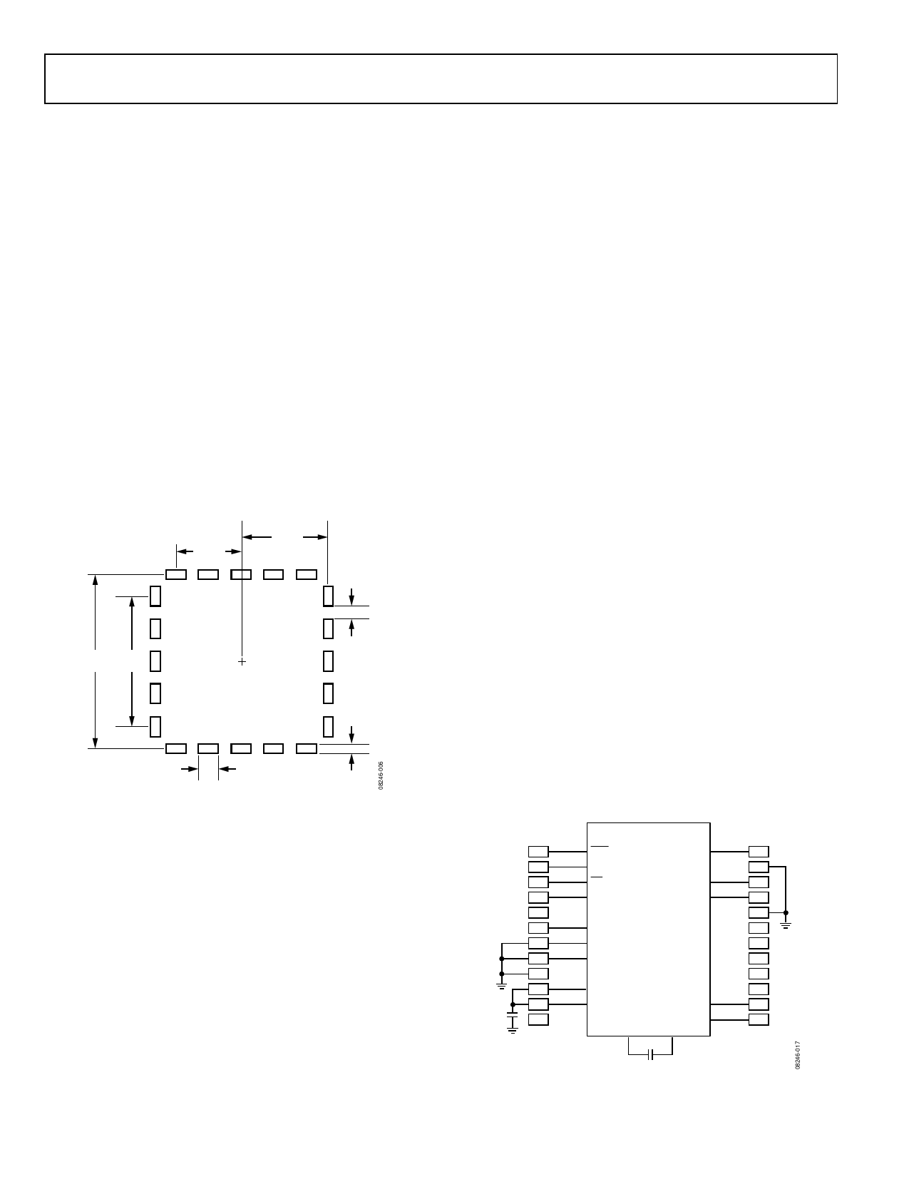
forces across the bottom of the package. Figure 18 provides a
PCB pad design example for this package style.
3.800
8×
5.0865
8×
0.773
16×
10.173 7.600
2×
4×
0.500
20×
1.127
20×
11mm × 11mm STACKED LGA PACKAGE
Figure 18. Recommended Pad Layout (Units in Millimeters)
BIAS OPTIMIZATION
Use the following steps to fine-tune the bias to an accuracy that
approaches the in-run bias stability, 0.007°/sec (1 σ).
1. Apply 5 V and wait 10 sec.
2. Set SENS_AVG[10:8] = 001 (DIN = 0xB901).
3. Set GLOB_CMD[1] = 1 (DIN = 0xBE02).
4. Collect GYRO_OUT data for 150 sec at a sample rate of
256 SPS.
5. Average data record.
6. Round to the nearest integer.
7. Multiply by −1.
8. Write to GYRO_OFF.
9. Update flash.
Set GLOB_CMD[3] = 1 (DIN = 0xBE08).
Wait for >50 ms and resume operation.
The Allan Variance curve in Figure 6 provides a trade-off
relationship between accuracy and averaging time. For example, an
average time of 1 second produce an accuracy of ~0.035 °/sec (1 σ).
INTERFACE PRINTED CIRCUIT BOARD (PCB)
The ADIS16265/PCBZ includes one ADIS16265BCCZ IC on a
1.2 inch × 1.3 inch PCB. The ADIS16260/PCBZ includes one
ADIS16260BCCZ on a 1.2 inch × 1.3 inch PCB. The interface
PCB simplifies the IC connection of these devices to an existing
processor system. The four mounting holes accommodate either
M2 (2 mm) or 2-56 machine screws. These boards are made of
IS410 material and are 0.063 inches thick. The second-level
assembly uses a SAC305-compatible solder composition, which
has a presolder reflow thickness of approximately 0.005 inches.
The pad pattern on these PCBs matches that shown in Figure 20.
J1 and J2 are dual-row, 2 mm (pitch) connectors that work with
a number of ribbon cable systems, including 3M Part Number
152212-0100-GB (ribbon crimp connector) and 3M Part Number
3625/12 (ribbon cable). The schematic and connector pin
assignments for the ADIS16260/PCBZ and the ADIS16265/PCBZ
are shown in Figure 19.
7
1
RST
1
2
SCLK
4
3
CS
4
2 DOUT
AUX ADC 13
1
2
12
AUX DAC
3
VREF 20
4
5
6
3 DIN
18
ADIS16260/
ADIS16265
5
6
7
GND
7
19
8
GND
8
9
9
16
10
VCC
10
11
17 VCC
DIO2 6
11
C1
12
5
DIO1
12
RATE FILT
14
15
C2
Figure 19. Electrical Schematic
Rev. D | Page 18 of 20
Share Link: 