ADM1021 View Datasheet(PDF) - Analog Devices
Part Name
Description
Manufacturer
ADM1021 Datasheet PDF : 12 Pages
| |||
ADM1021
ABSOLUTE MAXIMUM RATINGS*
Positive Supply Voltage (VDD) to GND . . . . . . . –0.3 V to +6 V
D+, ADD0, ADD1 . . . . . . . . . . . . . . . . –0.3 V to VDD + 0.3 V
D– to GND . . . . . . . . . . . . . . . . . . . . . . . . . . –0.3 V to +0.6 V
SCLK, SDATA, ALERT, STBY . . . . . . . . . . . . –0.3 V to +6 V
Input Current, SDATA . . . . . . . . . . . . . . . . –1 mA to +50 mA
Input Current, D– . . . . . . . . . . . . . . . . . . . . . . . . . . . . . ± 1 mA
ESD Rating, all pins (Human Body Model) . . . . . . . . 2000 V
Continuous Power Dissipation
Up to +70°C . . . . . . . . . . . . . . . . . . . . . . . . . . . . . 650 mW
Derating above +70°C . . . . . . . . . . . . . . . . . . . . 6.7 mW/°C
Operating Temperature Range . . . . . . . . . . –55°C to +125°C
Maximum Junction Temperature (TJ max) . . . . . . . . . +150°C
Storage Temperature Range . . . . . . . . . . . . –65°C to +150°C
Lead Temperature, Soldering
Vapor Phase 60 sec . . . . . . . . . . . . . . . . . . . . . . . . . +215°C
Infrared 15 sec . . . . . . . . . . . . . . . . . . . . . . . . . . . . . +200°C
*Stresses above those listed under Absolute Maximum Ratings may cause perma-
nent damage to the device. This is a stress rating only; functional operation of the
device at these or any other conditions above those indicated in the operational
section of this specification is not implied. Exposure to absolute maximum rating
conditions for extended periods may affect device reliability.
THERMAL CHARACTERISTICS
16-Lead QSOP Package: θJA = 150°C/Watt.
ORDERING GUIDE
Model
Temperature
Range
ADM1021ARQ 0°C to +85°C
Package
Package
Description Option
16-Lead QSOP RQ-16
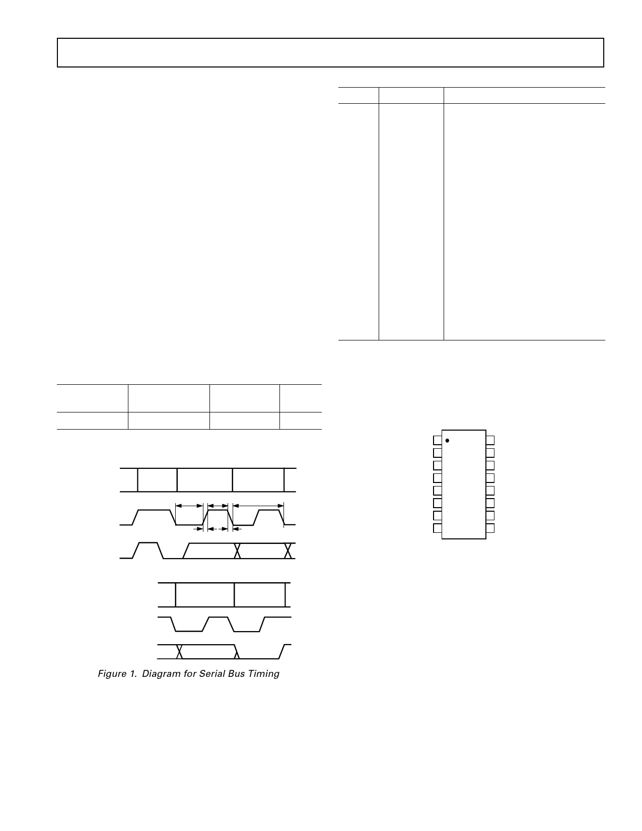
PROTOCOL
SCL
SDA
START
CONDITION
(S)
BIT 7
MSB
(A7)
tLOW tHIGH
BIT 6
(A6)
1/fSCL
tR
tF
PIN FUNCTION DESCRIPTIONS
Pin No. Mnemonic Description
1, 16
2
3
4
5, 9, 13
6
7, 8
10
11
12
14
15
TEST
VDD
D+
D–
NC
ADD1
GND
ADD0
ALERT
SDATA
SCLK
STBY
Test pin for factory use only. See
note.
Positive supply, +3 V to +5.5 V.
Positive connection to remote tem-
perature sensor.
Negative connection to remote tem-
perature sensor.
No Connect.
Three-state logic input, higher bit of
device address.
Supply 0 V connection.
Three-state logic input, lower bit of
device address.
Open-drain logic output used as
interrupt or SMBus alert.
Logic input/output, SMBus serial
data. Open-drain output.
Logic input, SMBus serial clock.
Logic input selecting normal opera-
tion (high) or standby mode (low).
NOTE
Pins 1 and 16 are reserved for test purposes. Ideally these pins should be left
unconnected. If routing through these pins is required, then both should be at
the same potential (i.e., connected together).
PIN CONFIGURATION
TEST 1
16 TEST
VDD 2
15 STBY
D+ 3
14 SCLK
D– 4 ADM1021 13 NC
TOP VIEW
NC 5 (Not to Scale) 12 SDATA
ADD1 6
11 ALERT
GND 7
10 ADD0
GND 8
9 NC
NC = NO CONNECT
PROTOCOL
SCL
BIT 0
LSB
(R/W)
ACKNOWLEDGE
(A)
STOP
CONDITION
(P)
SDA
Figure 1. Diagram for Serial Bus Timing
REV. 0
–3–
Share Link: 