ADM3251E_VE View Datasheet(PDF) - Analog Devices
Part Name
Description
Manufacturer
ADM3251E_VE Datasheet PDF : 16 Pages
| |||
ADM3251E
THEORY OF OPERATION
The ADM3251E is a high speed, 2.5 kV fully isolated, single-
channel RS-232 transceiver device that operates from a single
power supply.
The internal circuitry consists of the following main sections:
• Isolation of power and data
• A charge pump voltage converter
• A 5.0 V logic to EIA/TIA-232E transmitter
• A EIA/TIA-232E to 5.0 V logic receiver
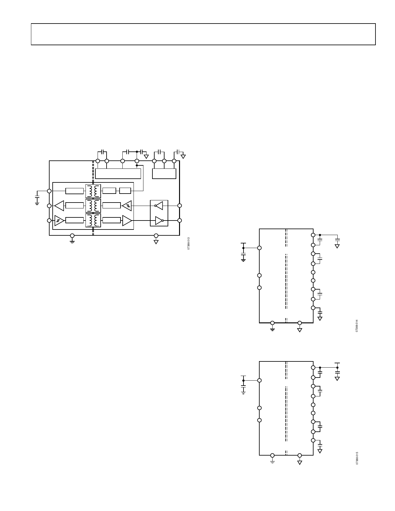
C1
0.1µF
16V
C3
0.1µF
10V 0.1µF
C2
0.1µF
16V
C4
0.1µF
16V
ADM3251E
VCC
0.1µF
ROUT
TIN
OSC
DECODE
ENCODE
C1+ C1– V+ VISO
VOLTAGE
DOUBLER
C2+ C2– V–
VOLTAGE
INVERTER
RECT REG
ENCODE
DECODE
R
RIN*
T
TOUT
The TIN pin accepts TTL/CMOS input levels. The driver input
signal that is applied to the TIN pin is referenced to logic ground
(GND). It is coupled across the isolation barrier, inverted, and
then appears at the transceiver section, referenced to isolated
ground (GNDISO). Similarly, the receiver input (RIN) accepts
RS-232 signal levels that are referenced to isolated ground.
The RIN input is inverted and coupled across the isolation
barrier to appear at the ROUT pin, referenced to logic ground.
The digital signals are transmitted across the isolation barrier
using iCoupler technology. Chip-scale transformer windings
couple the digital signals magnetically from one side of the
barrier to the other. Digital inputs are encoded into waveforms
that are capable of exciting the primary transformer of the winding.
At the secondary winding, the induced waveforms are decoded
into the binary value that was originally transmitted.
There is hysteresis in the VCC input voltage detect circuit.
Once the dc-to-dc converter is active, the input voltage
must be decreased below the turn-on threshold to disable
the converter. This feature ensures that the converter does
not go into oscillation due to noisy input power.
GND
GNDISO
*INTERNAL 5kΩ PULL-DOWN RESISTOR ON THE RS-232 INPUT.
Figure 13. Functional Block Diagram
ISOLATION OF POWER AND DATA
The ADM3251E incorporates a dc-to-dc converter section,
which works on principles that are common to most modern
power supply designs. VCC power is supplied to an oscillating
circuit that switches current into a chip-scale air core transformer.
Power is transferred to the secondary side, where it is rectified
to a high dc voltage. The power is then linearly regulated to
about 5.0 V and supplied to the secondary side data section
and to the VISO pin. The VISO pin should not be used to power
external circuitry.
Because the oscillator runs at a constant high frequency
independent of the load, excess power is internally dissipated
in the output voltage regulation process. Limited space for
transformer coils and components also adds to internal power
dissipation. This results in low power conversion efficiency.
The ADM3251E can be operated with the dc-to-dc converter
enabled or disabled. The internal dc-to-dc converter state of the
ADM3251E is controlled by the input VCC voltage. In normal
operating mode, VCC is set between 4.5 V and 5.5 V and the
internal dc-to-dc converter is enabled. To disable the dc-to-dc
converter, lower VCC to a value between 3.0 V and 3.7 V. In this
mode, the user must externally supply isolated power to the
VISO pin. An isolated secondary side voltage of between 3.0 V
and 5.5 V and a secondary side input current, IISO, of 12 mA
(maximum) is required on the VISO pin. The signal channels of
the ADM3251E then continue to operate normally.
4.5V TO 5.5V
0.1µF
VISO
V+
VCC ADM3251E
C1+
C1–
C3
+ 0.1µF
+ 0.1µF
10V
+ C1
0.1µF
16V
CMOS OUTPUT ROUT
CMOS INPUT TIN
TOUT
RIN
C2+
C2–
EIA/TIA-232E OUTPUT
EIA/TIA-232E INPUT
+ C2
0.1µF
16V
GND
ISOLATION
BARRIER
V–
GNDISO
C4
+ 0.1µF
16V
Figure 14. Typical Operating Circuit with the DC-to-DC Converter Enabled
(VCC = 4.5 V to 5.5 V)
3.0V TO 3.7V
0.1µF
VISO
V+
VCC ADM3251E
C1+
C1–
3.0V TO 5.5V
ISOLATED SUPPLY
C3
+ 0.1µF
+
0.1µF
10V
+ C1
0.1µF
16V
CMOS OUTPUT ROUT
CMOS INPUT TIN
TOUT
RIN
C2+
C2–
EIA/TIA-232E OUTPUT
EIA/TIA-232E INPUT
+ C2
0.1µF
16V
GND
ISOLATION
BARRIER
V–
GNDISO
C4
+ 0.1µF
16V
Figure 15. Typical Operating Circuit with the DC-to-DC Converter Disabled
(VCC = 3.0 V to 3.7 V)
Rev. E | Page 11 of 16
Share Link: 