ADM3251E_VE View Datasheet(PDF) - Analog Devices
Part Name
Description
Manufacturer
ADM3251E_VE Datasheet PDF : 16 Pages
| |||
ADM3251E
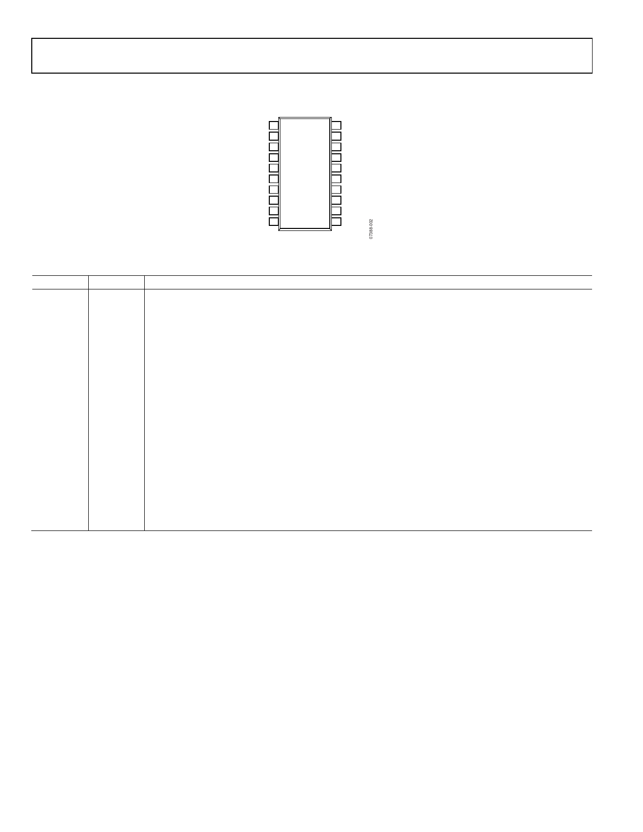
PIN CONFIGURATION AND FUNCTION DESCRIPTIONS
NC 1
VCC 2
VCC 3
GND 4
GND 5
GND 6
GND 7
ROUT 8
TIN 9
GND 10
ADM3251E
TOP VIEW
(Not to Scale)
20 VISO
19 V+
18 C1+
17 C1–
16 TOUT
15 RIN
14 C2+
13 C2–
12 V–
11 GNDISO
NC = NO CONNECT
Figure 2. Pin Configuration
Table 8. Pin Function Descriptions
Pin No.
Mnemonic Description
1
NC
No Connect. This pin should always remain unconnected.
2, 3
VCC
Power Supply Input. A 0.1 μF decoupling capacitor is required between VCC and ground. When a voltage
between 4.5 V and 5.5 V is applied to the VCC pin, the integrated dc-to-dc converter is enabled. If this voltage is
lowered to between 3.0 V and 3.7 V, the integrated dc-to-dc converter is disabled.
4, 5, 6, 7, 10 GND
Ground.
8
ROUT
Receiver Output. This pin outputs CMOS logic levels.
9
TIN
Transmitter (Driver) Input. This pin accepts TTL/CMOS levels.
11
GNDISO
Ground Reference for Isolator Primary Side.
12
V−
Internally Generated Negative Supply.
13, 14
C2−, C2+
Positive and Negative Connections for Charge Pump Capacitors. External Capacitor C2 is connected between
these pins; a 0.1 μF capacitor is recommended, but larger capacitors up to 10 μF can be used.
15
RIN
Receiver Input. This input accepts RS-232 signal levels.
16
TOUT
Transmitter (Driver) Output. This outputs RS-232 signal levels.
17, 18
C1−, C1+
Positive and Negative Connections for Charge Pump Capacitors. External Capacitor C1 is connected between
these pins; a 0.1 μF capacitor is recommended, but larger capacitors up to 10 μF can be used.
19
V+
Internally Generated Positive Supply.
20
VISO
Isolated Supply Voltage for Isolator Secondary Side. A 0.1 μF decoupling capacitor is required between VISO and
ground. When the integrated dc-to-dc converter is enabled, the VISO pin should not be used to power external
circuitry. If the integrated dc-to-dc converter is disabled, power the secondary side by applying a voltage in the
range of 3.0 V to 5.5 V to this pin.
Rev. E | Page 8 of 16
Share Link: 