AHA4013B View Datasheet(PDF) - Unspecified
Part Name
Description
Manufacturer
AHA4013B Datasheet PDF : 28 Pages
| |||
Advanced Hardware Architectures, Inc.
2.5 DATA FLOW
The device is first initialized for various
programmable parameters including: Erasure
Multiplier, Error Threshold, Number of Check
bytes, Number of Message bytes per block, Block
Length and a Control byte. Following this six-byte
initialization, the device may be used to encode,
decode or pass-through multiple blocks of data. The
device requires reinitialization when the parameters
are changed or a reset is required.
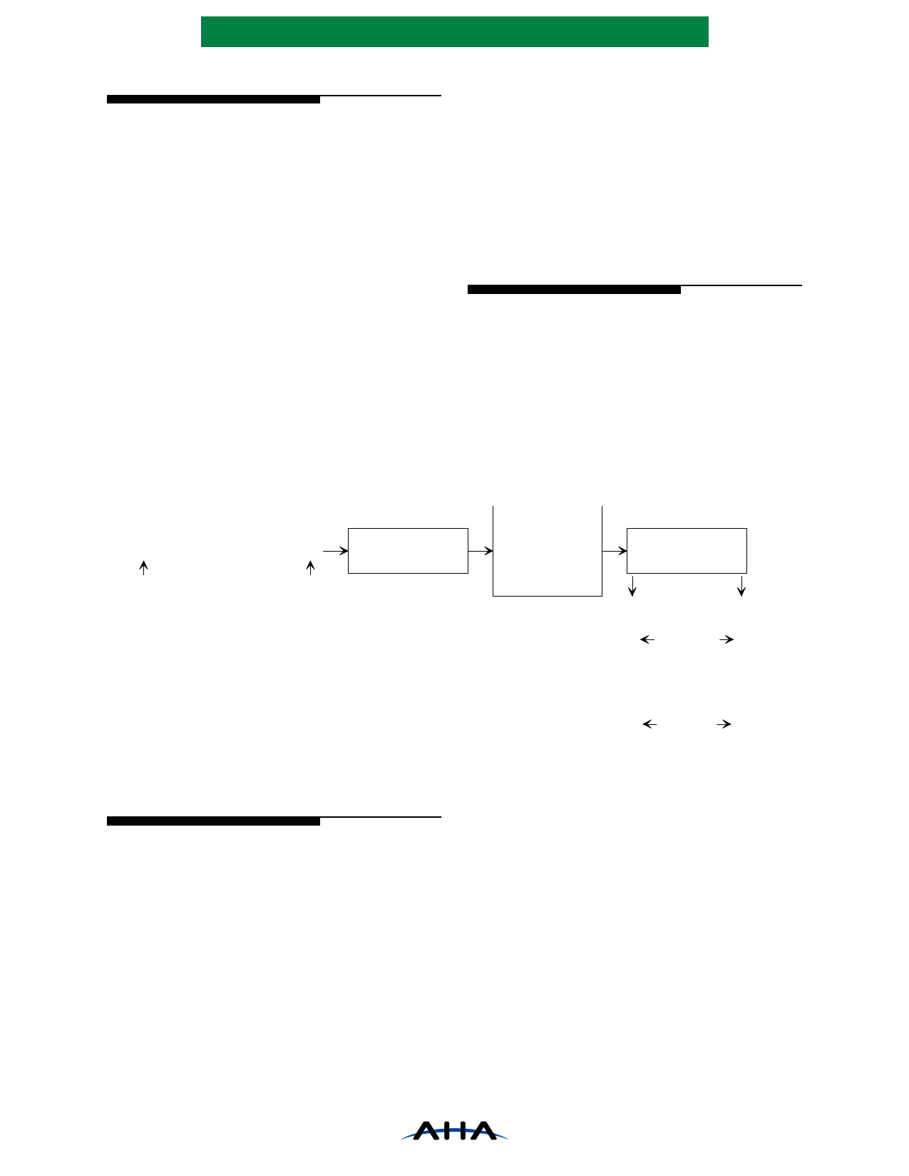
The device processes data as “blocks”
containing Message and Check Bytes. Order of
input bytes must be first message byte XK−1 through
last message byte X0, followed by first check byte
YR−1 through last check byte Y0. The device
processes the block in this manner:
- a block is clocked into the Input Buffer;
- transferred into the ECC module;
- passed to the Output Buffer in the reverse order
from what was received at the Input Port; and
Figure 3: Data Input and Output Order
- clocked out through the Output Port via the
Output Buffer. Consecutive blocks may be
input into the Input Buffer while the Output
Buffer is being emptied.
Data is available through the Output Port in
forward or reverse order. Forward order clocks out
the block the same as input and reverse order clocks
the check byte Y0 through check bytes YR−1
followed by message byte X0 through message byte
XK−1.
2.5.1 SHORTENED BLOCKS
This device allows for shortened RS blocks,
thus not requiring zero padding when decoding.
During encoding, conversely, zero padding is not
performed. When the device is programmed to
decode a block of less than 255 Bytes, only the
message bytes followed by check bytes are sent.
Prepending with zero value bytes to fill out the
block to 255 Bytes is not required.
Y0 Y1 . . . YR-2 YR-1 X0 X1 . . . X K-2 X K-1
Last
First
Byte
Byte
In
In
INPUT
BUFFER
ECC
Core
OUTPUT
BUFFER
Data Available
Reverse Order
Data Available
Forward Order
X...K-1
Last Byte Out
Y...0
X0
YR-1
YR... -1
X...0
Y0
First Byte Out X K-1
2.6 RESET AND INITIALIZATION
SEQUENCE
Reset and initialization first requires pulling the
RSTN low signal for at least two clocks while the
DSIN and DSON signals are held inactive, i.e., high
Following this sequence, the six internal
registers, referred to as “Initialization Registers” are
strobed by DSIN. These bytes are loaded in order of
1 through 6.
The RSTN must be active low for at least two
clocks before the first initialization byte is strobed
in and remain active for at least one clock after the
final byte. RSTN must be high for at least two
clocks before the first message byte can be strobed
into the device. For a detailed timing diagram, see
Figure 7: Initialization and Reset Timing.
The chip must be reset and initialized any time
a reset is necessary.
Caveat: All six registers must be initialized
correctly for proper operation of the chip. The
device has no provisions for reading back
Initialization Register settings. This sequence must
be used if the device needs to be reset or any one
register needs updating, i.e., all registers must be
reinitialized for a change to any one register.
PS4013B-0600
Page 5 of 24
Share Link: 