MCM64AF32SG15 View Datasheet(PDF) - Motorola => Freescale
Part Name
Description
Manufacturer
MCM64AF32SG15 Datasheet PDF : 12 Pages
| |||
CAPACITANCE (f = 1.0 MHz, dV = 3.0 V, TA = 25°C, Periodically Sampled Rather Than 100% Tested)
Parameter
Symbol
Input Capacitance
(TWE, CALE, CWE0 – CWE7)
Cin
(A5 – A17)
(CAA3, CAA4, CAB3, CAB4)
(COE)
Input/Output Capacitance
(DQ0 – DQ63)
(TIO0 – TIO7)
CI/O
Max
Unit
8
pF
14
26
50
8
pF
10
DATA RAMs AC OPERATING CONDITIONS AND CHARACTERISTICS
(VCC = 3.3 V ± 5%, TA = 0 to + 70°C, Unless Otherwise Noted)
Input Timing Measurement Reference Level . . . . . . . . . . . . . . . 1.5 V
Input Pulse Levels . . . . . . . . . . . . . . . . . . . . . . . . . . . . . . . . . 0 to 3.0 V
Input Rise/Fall Time . . . . . . . . . . . . . . . . . . . . . . . . . . . . . . . . . . . . 3 ns
Output Timing Measurement Reference Level . . . . . . . . . . . . . 1.5 V
Output Load . . . . . . . . . . . . . . . . Figure 1A Unless Otherwise Noted
DATA RAMs READ CYCLE (See Note 1)
–15
Parameter
Symbol
Min
Max
Unit
Notes
Read Cycle Time
tAVAV
15
—
ns
2
Address Access Time (CAAx, CABx)
tAVQV
—
15
ns
Latched Address Access Time (A5 – A17)
tLAVQV
—
22
ns
Latched Address to CALE Low Setup Time
tAVCALL
4
—
ns
Latched Address to CALE Low Hold Time
tCALAX
3
—
ns
Enable Access Time
tELQV
—
15
ns
3
Output Enable Access Time
tGLQV
—
8
ns
Output Hold from Address Change
tAXQX
4
—
ns
6
Enable Low to Output Active
tELQX
4
—
ns
4, 5, 6
Enable High to Output High–Z
tEHQZ
0
8
ns
4, 5, 6
Output Enable Low to Output Active
tGLQX
0
—
ns
4, 5, 6
Output Enable High to Output High–Z
tGHQZ
0
7
ns
4, 5, 6
Power Up Time
tELICCH
0
—
ns
Power Down Time
tEHICCL
—
15
ns
NOTES:
1. CWE is high for read cycle.
2. All timings are referenced from the last valid address to the first address transition.
3. Addresses valid prior to or coincident with CS going low.
4. At any given voltage and temperature, tGHQZ (max) is less than tGLQX (min), both for a
given device and from device to device.
5. Transition is measured ± 500 mV from steady–state voltage with load of Figure 1B.
6. This parameter is sampled and not 100% tested.
7. Device is continuously selected (COE = VIL).
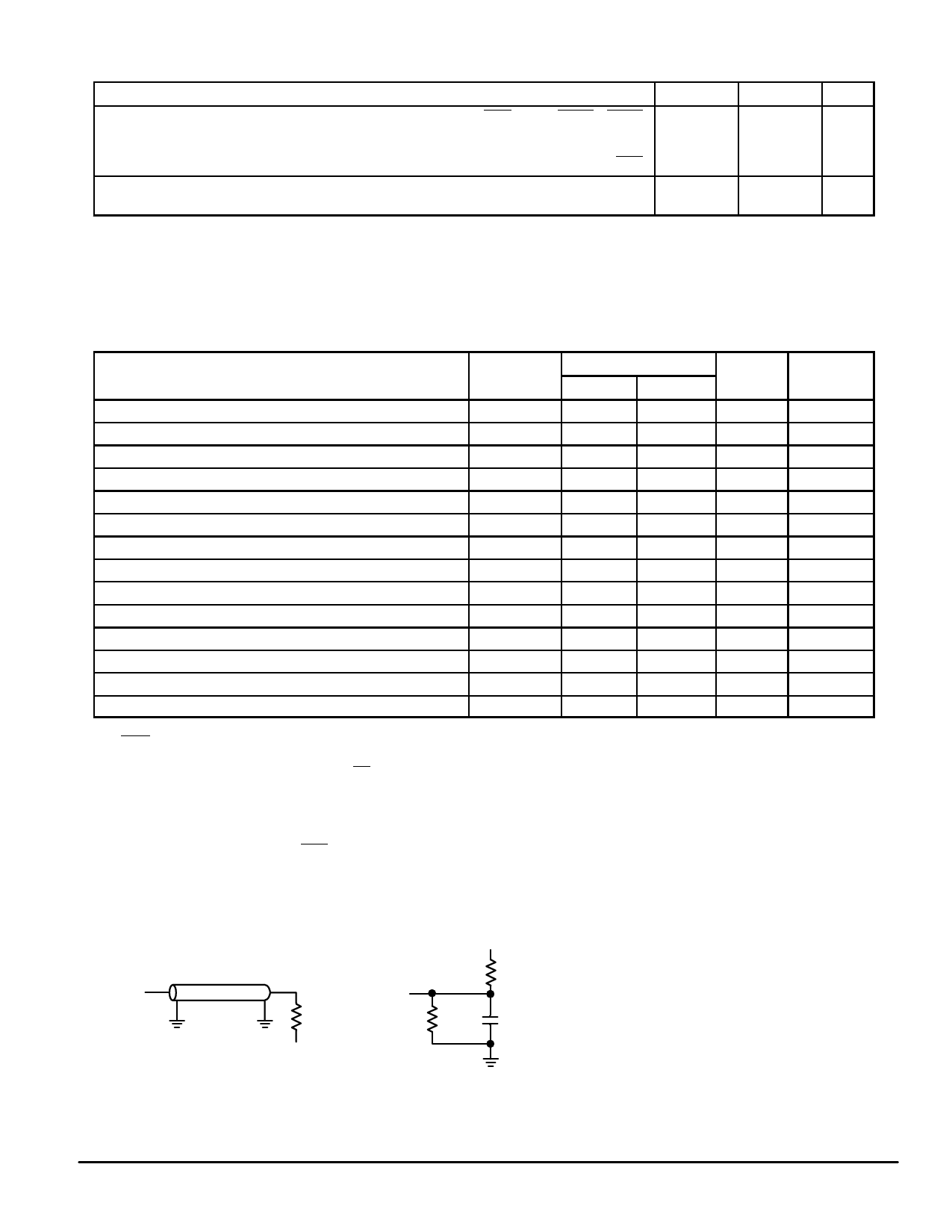
OUTPUT
AC TEST LOADS
Z0 = 50 Ω
50 Ω
VL = 1.5 V
OUTPUT
353 Ω
+ 3.3 V
319 Ω
5 pF
Figure 1A
Figure 1B
TIMING LIMITS
The table of timing values shows either a
minimum or a maximum limit for each param-
eter. Input requirements are specified from
the external system point of view. Thus, ad-
dress setup time is shown as a minimum
since the system must supply at least that
much time (even though most devices do not
require it). On the other hand, responses from
the memory are specified from the device
point of view. Thus, the access time is shown
as a maximum since the device never pro-
vides data later than that time.
MCM64AF32
6
MOTOROLA FAST SRAM
Share Link: 