MCM64AF32SG15 View Datasheet(PDF) - Motorola => Freescale
Part Name
Description
Manufacturer
MCM64AF32SG15 Datasheet PDF : 12 Pages
| |||
TAG RAM AC OPERATING CONDITIONS AND CHARACTERISTICS
(VCC = 5.0 V ± 5%, TA = 0 to + 70°C, Unless Otherwise Noted)
Input Timing Measurement Reference Level . . . . . . . . . . . . . . . 1.5 V
Input Pulse Levels . . . . . . . . . . . . . . . . . . . . . . . . . . . . . . . . . 0 to 3.0 V
Input Rise/Fall Time . . . . . . . . . . . . . . . . . . . . . . . . . . . . . . . . . . . . 3 ns
Output Timing Measurement Reference Level . . . . . . . . . . . . . 1.5 V
Output Load . . . . . . . . . . . . . . . . Figure 1A Unless Otherwise Noted
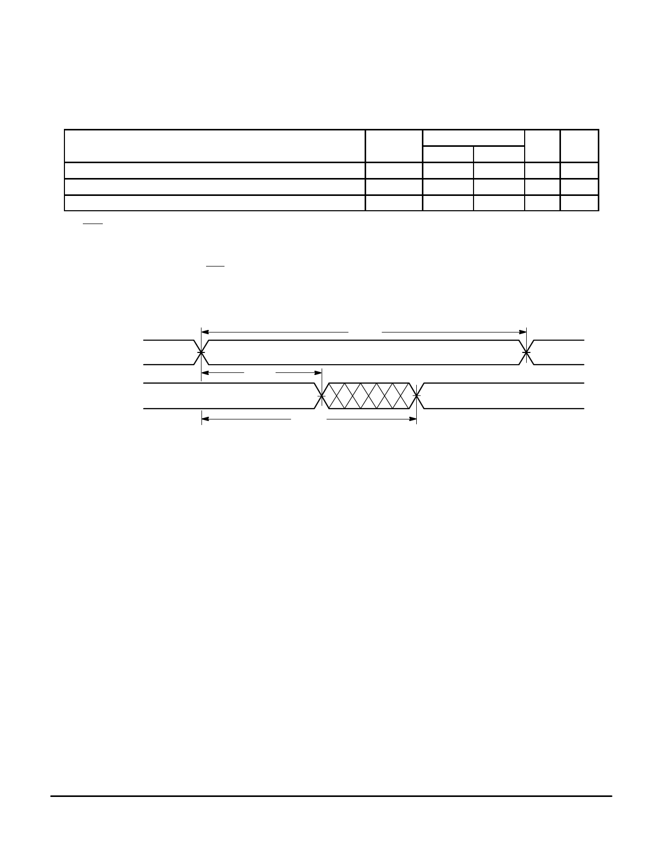
TAG RAM READ CYCLE (See Notes 1 and 5)
Parameter
Symbol
Read Cycle Time
tAVAV
Address Access Time
tAVQV
Output Hold from Address Change
tAXQX
NOTES:
1. CWE is high for read cycle.
2. All timings are referenced from the last valid address to the first address transition.
3. Transition is measured ± 500 mV from steady–state voltage with load of Figure 1B.
4. This parameter is sampled and not 100% tested.
5. Device is continuously selected (COE = VIL).
– 15
Min
Max
15
—
—
15
4
—
Unit Notes
ns
2
ns
ns
3, 4
A5 – A17
Q (DATA OUT)
TAG RAM READ CYCLE (See Note 5)
tAVAV
tAXQX
PREVIOUS DATA VALID
tAVQV
DATA VALID
MOTOROLA FAST SRAM
MCM64AF32
9
Share Link: 