CYM1841A View Datasheet(PDF) - Cypress Semiconductor
Part Name
Description
Manufacturer
CYM1841A Datasheet PDF : 11 Pages
| |||
fax id: 2017
CYM1841A
CYM1841C
Features
• High-density 8-megabit SRAM module
• 32-bit standard footprint supports densities from 16K
x 32 through 1M x 32
• High-speed CMOS SRAMs
— Access time of 12 ns
• Low active power
— 5.3W (max.) at 25 ns
• SMD technology
• TTL-compatible inputs and outputs
• Low profile
— Max. height of 0.58 in.
• Available in ZIP, SIMM, and angled SIMM footprint
• 72-pin SIMM version compatible with 1M x 32
(CYM1851)
Functional Description
The CYM1841A/1841C are high-performance 8-megabit stat-
ic RAM modules organized as 256K words by 32 bits. This
module is constructed from eight 256K x 4 SRAMs in SOJ
packages mounted on an epoxy laminate board with pins. Four
chip selects (CS1, CS2, CS3, CS4) are used to independently
enable the four bytes. Reading or writing can be executed on
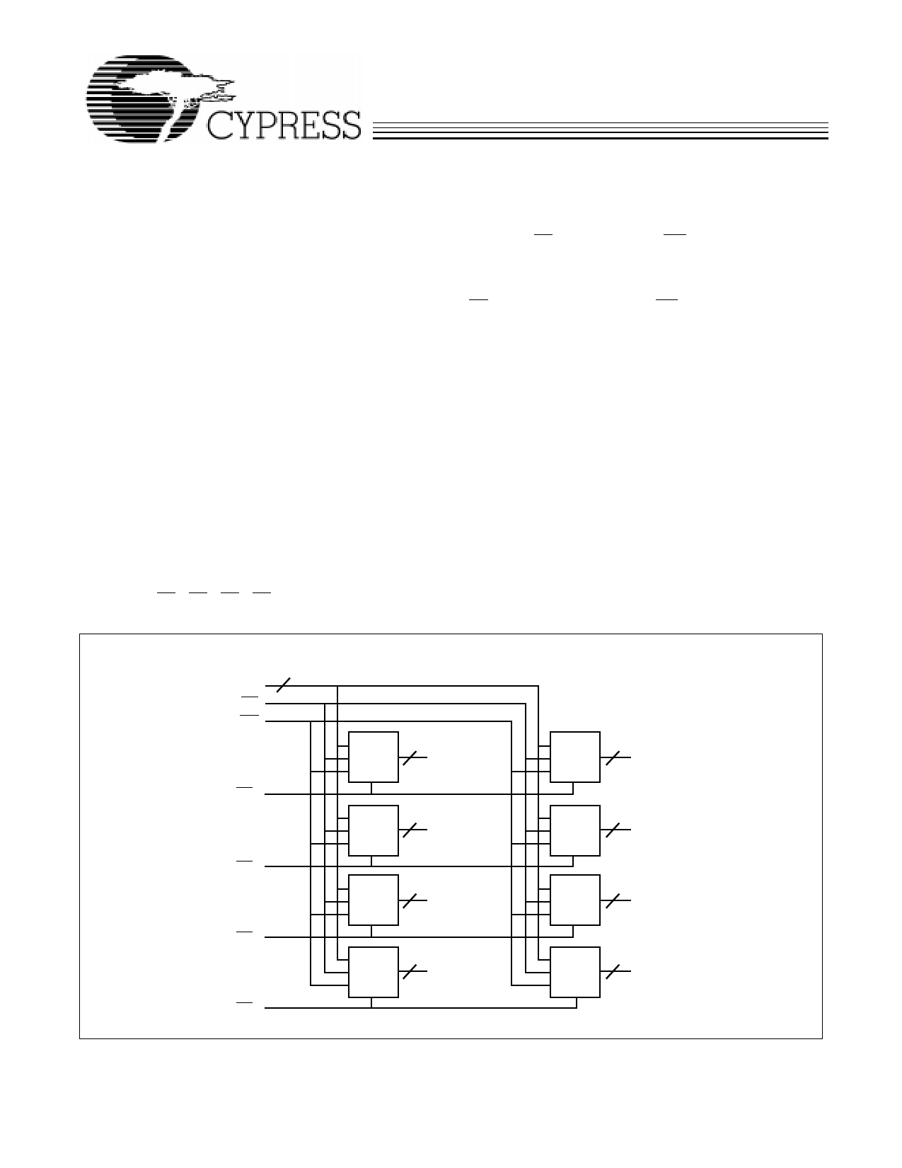
Logic Block Diagram
A0 –A17
18
OE
WE
256K x 32 Static RAM Module
individual bytes or any combination of multiple bytes through
proper use of selects.
Writing to each byte is accomplished when the appropriate
chip select (CS) and write enable (WE) inputs are both LOW.
Data on the input/output pins (I/O) is written into the mem-
ory location specified on the address pins (A0 through A17).
Reading the device is accomplished by taking the chip select
(CS) LOW while write enable (WE) remains HIGH. Under
these conditions, the contents of the memory location speci-
fied on the address pins will appear on the data input/output
pins (I/O).
The data input/output pins stay at the high-impedance state
when write enable is LOW or the appropriate chip selects are
HIGH.
Two pins (PD0 and PD1) are used to identify module mem-
ory density in applications where alternate versions of the
JEDEC-standard modules can be interchanged.
The CYM1841A and CYM1841C are 100% pin, package, and
electrically identical. The CYM1841A utilizes corner power
and ground SRAMs, the CYM1841C utilizes center power and
ground SRAMs.
A 72-pin SIMM is offered for compatibility with the 1M x 32
CYM1851. This version is socket upgradable to the CYM1851.
Both the 64-pin and 72-pin SIMM modules are available with
either tin-lead or 10 micro-inches of gold flash on the edge
contacts.
PD0 – GND
PD1 – GND
PD2 – OPEN (72-pin only)
PD3 – OPEN (72-pin only)
256K x 4
SRAM 4
I/O0 – I/O3
256K x 4
SRAM 4
I/O4 – I/O7
CS1
256K x 4
SRAM 4
I/O8 – I/O11
256K x 4
SRAM 4
I/O12 – I/O15
CS2
256K x 4
SRAM 4
I/O16 – I/O19
256K x 4
SRAM 4
I/O20 – I/O23
CS3
256K x 4
SRAM 4
I/O24 – I/O27
256K x 4
SRAM 4
I/O28 – I/O31
CS4
1841A–1
Cypress Semiconductor Corporation • 3901 North First Street • San Jose • CA 95134 • 408-943-2600
September 1989 – Revised December 10, 1997
Share Link: 