CYM1841A View Datasheet(PDF) - Cypress Semiconductor
Part Name
Description
Manufacturer
CYM1841A Datasheet PDF : 11 Pages
| |||
CYM1841A
CYM1841C
Maximum Ratings
(Above which the useful life may be impaired. For user guide-
lines, not tested.)
Storage Temperature ..................................... –55°C to +125°C
Ambient Temperature with
Power Applied .................................................... –10°C to +85°C
Supply Voltage to Ground Potential..................–0.5V to +7.0V
DC Voltage Applied to Outputs
in High Z State ..................................................... –0.5V to +7.0V
DC Input Voltage ................................................. –0.5V to +7.0V
Operating Range
Range
Commercial
Ambient
Temperature
0°C to +70°C
VCC
5V ± 10%
Electrical Characteristics Over the Operating Range
Parameter
Description
VOH
Output HIGH Voltage
VOL
Output LOW Voltage
VIH
Input HIGH Voltage
VIL
Input LOW Voltage
IIX
Input Leakage Current
IOZ
Output Leakage
Current
ICC
VCC Operating
Supply Current
ISB1
Automatic CS Power-
Down Current[1]
ISB2
Automatic CS Power-
Down Current[1]
Test Conditions
VCC = Min., IOH = –4.0 mA
VCC = Min., IOL = 8.0 mA
GND < VI < VCC
GND < VO < VCC,
Output Disabled
VCC = Max., IOUT = 0 mA,
CS < VIL
Max. VCC, CS > VIH,
Min. Duty Cycle = 100%
Max. VCC, CS > VCC - 0.2V,
VIN > VCC – 0.2V,
or VIN < 0.2V
1841C-12
1841C-15
Min. Max.
2.4
0.4
2.2 VCC
–0.5 0.8
–16 +16
–10 +10
1841A-20 1841A-25, 35, 45
1841C-20 1841C-25, 35, 45
Min. Max. Min. Max. Unit
2.4
2.4
V
0.4
0.4
V
2.2 VCC 2.2
VCC
V
–0.5 0.8 –0.5 0.8
V
–16 +16 –16 +16 µA
–10 +10 –10 +10 µA
1600
1120
960 mA
480
480
480 mA
240
120
120 mA
Capacitance[2]
Parameter
Description
Test Conditions
Max.
Unit
CIN
COUT
Input Capacitance[3]
Output Capacitance
TA = 25°C, f = 1 MHz,
VCC = 5.0V
70/20
pF
20
pF
Notes:
1. A pull-up resistor to VCC on the CS input is required to keep the device deselected during VCC power-up, otherwise ISB will exceed values given.
2. Tested on a sample basis.
3. 20 pF on CS, 70 pF all others.
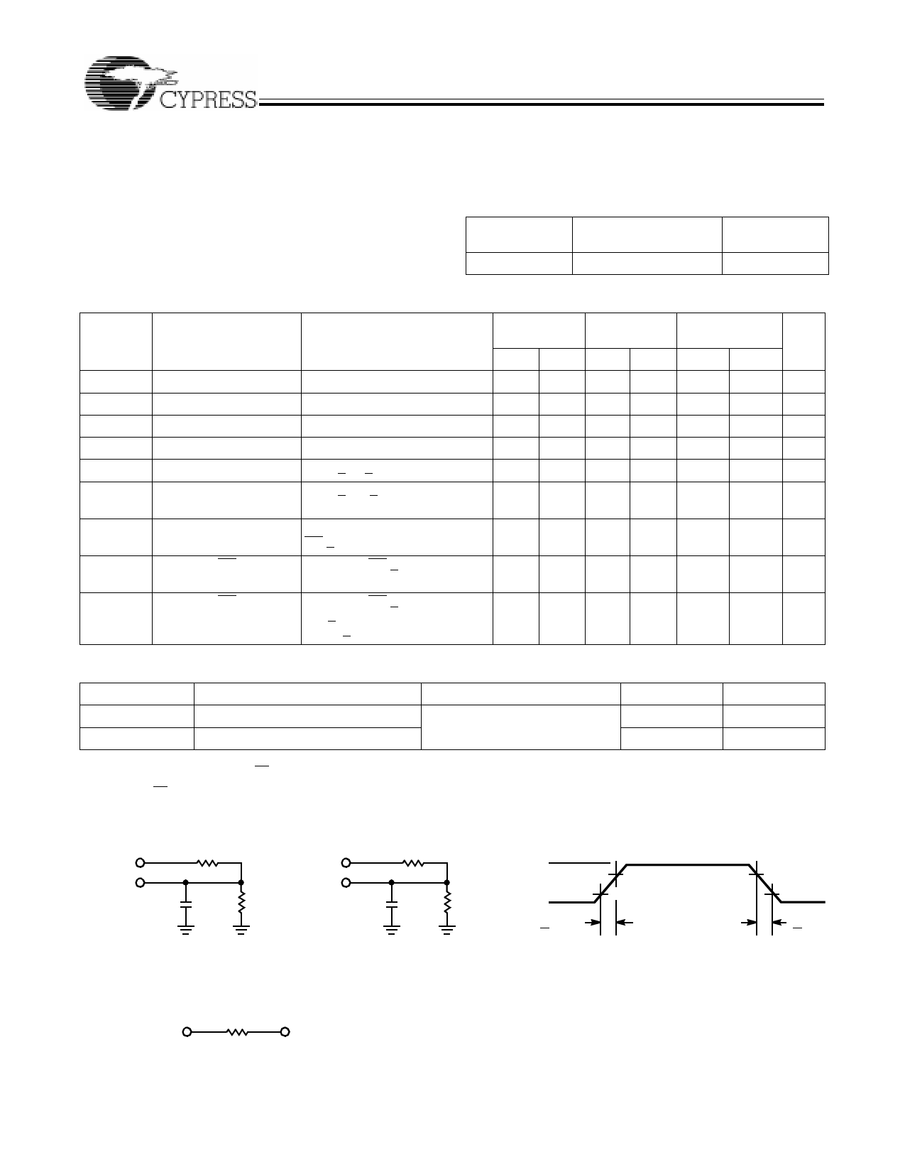
AC Test Loads and Waveforms
R1481 Ω
5V
OUTPUT
30 pF
INCLUDING
JIG AND
SCOPE
(a)
R1481 Ω
5V
R2 OUTPUT
255Ω
5 pF
R2
255Ω
INCLUDING
JIG AND
SCOPE
(b)
1841A–4
3.0V
GND
< 5 ns
ALL INPUT PULSES
90%
10%
90%
10%
< 5 ns
1841A–5
Equivalent to: THÉVENIN EQUIVALENT
OUTPUT
167Ω
1.73V
3
Share Link: 