CYM1841A View Datasheet(PDF) - Cypress Semiconductor
Part Name
Description
Manufacturer
CYM1841A Datasheet PDF : 11 Pages
| |||
CYM1841A
CYM1841C
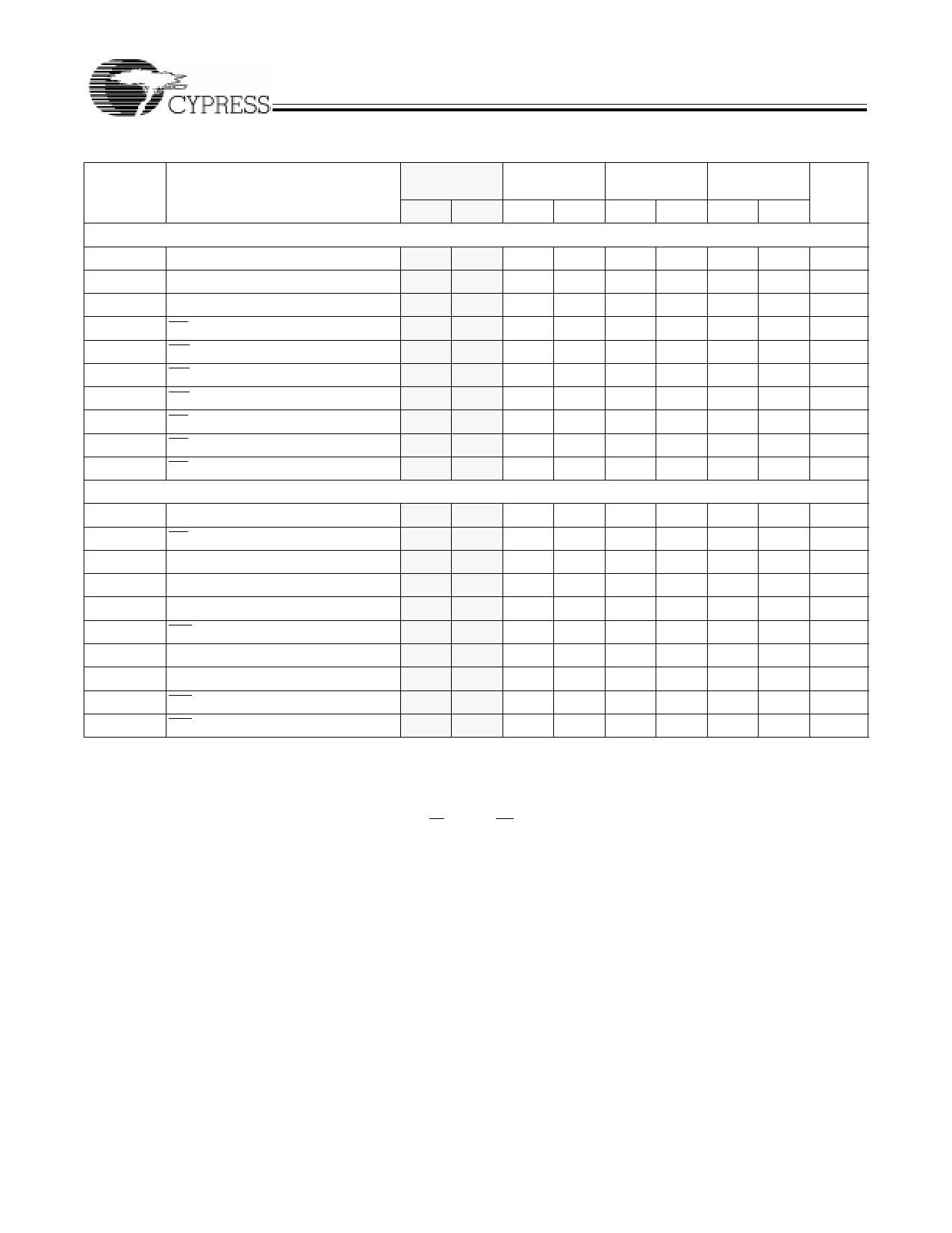
Switching Characteristics Over the Operating Range[4]
1841C-12
1841C-15
1841A-20
1841C-20
1841A-25
1841C-25
Parameter
Description
Min. Max. Min. Max. Min. Max. Min. Max. Unit
READ CYCLE
tRC
Read Cycle Time
12
15
20
25
ns
tAA
Address to Data Valid
12
15
20
25
ns
tOHA
Output Hold from Address Change
3
3
3
3
ns
tACS
CS LOW to Data Valid
12
15
20
25
ns
tDOE
OE LOW to Data Valid
7
8
13
15
ns
tLZOE
OE LOW to Low Z
0
0
0
0
ns
tHZOE
tLZCS
tHZCS
OE HIGH to High Z
CS LOW to Low Z[5]
CS HIGH to High Z[5, 6]
7
8
15
15
ns
3
3
10
10
ns
7
8
20
20
ns
tPD
CS HIGH to Power-Down
WRITE CYCLE[7]
12
15
20
25
tWC
Write Cycle Time
12
15
20
25
ns
tSCS
CS LOW to Write End
9
10
15
20
ns
tAW
Address Set-Up to Write End
9
10
18
20
ns
tHA
Address Hold from Write End
0
0
0
0
ns
tSA
Address Set-Up to Write Start
2
2
2
2
ns
tPWE
WE Pulse Width
10
13
15
20
ns
tSD
Data Set-Up to Write End
7
8
13
15
ns
tHD
Data Hold from Write End
1
1
2
2
ns
tLZWE
tHZWE
WE HIGH to Low Z
WE LOW to High Z[6]
0
0
0
0
ns
0
5
0
7
0
15
0
15
ns
Shaded area contains preliminary information.
Notes:
4. Test conditions assume signal transition times of 5 ns or less, timing reference levels of 1.5V, input pulse levels of 0 to 3.0V, and output loading of the specified
IOL/IOH and 30-pF load capacitance.
5. At any given temperature and voltage condition, tHZCS is less than tLZCS for any given device. These parameters are guaranteed by design and not 100% tested.
6. tHZCS and tHZWE are specified with CL = 5 pF as in part (b) of AC Test Loads and Waveforms. Transition is measured ±500 mV from steady-state voltage.
7. The internal write time of the memory is defined by the overlap of CS LOW and WE LOW. Both signals must be LOW to initiate a write and either signal can
terminate a write by going HIGH. The data input set-up and hold timing should be referenced to the rising edge of the signal that terminates the write.
4
Share Link: 