CY7C1366A View Datasheet(PDF) - Cypress Semiconductor
Part Name
Description
Manufacturer
CY7C1366A Datasheet PDF : 27 Pages
| |||
CY7C1366A/GVT71256C36
CY7C1367A/GVT71512C18
256K X 36 Pin Descriptions
X36 PBGA Pins
4P
4N
2A, 3A, 5A, 6A, 3B,
5B, 6B, 2C, 3C, 5C,
6C, 2R, 6R, 3T, 4T,
5T
5L
5G
3G
3L
4M
4H
4K
4E
2B
(not available for
PBGA)
4F
4G
4A
4B
3R
7T
X36 QFP Pins
37
36
35, 34, 33, 32,
100, 99, 82, 81,
44, 45, 46, 47,
48, 49, 50
92 (T Version)
43 (TA Version)
93
94
95
96
87
88
89
98
97
92 (for TA
Version only)
86
83
84
85
31
64
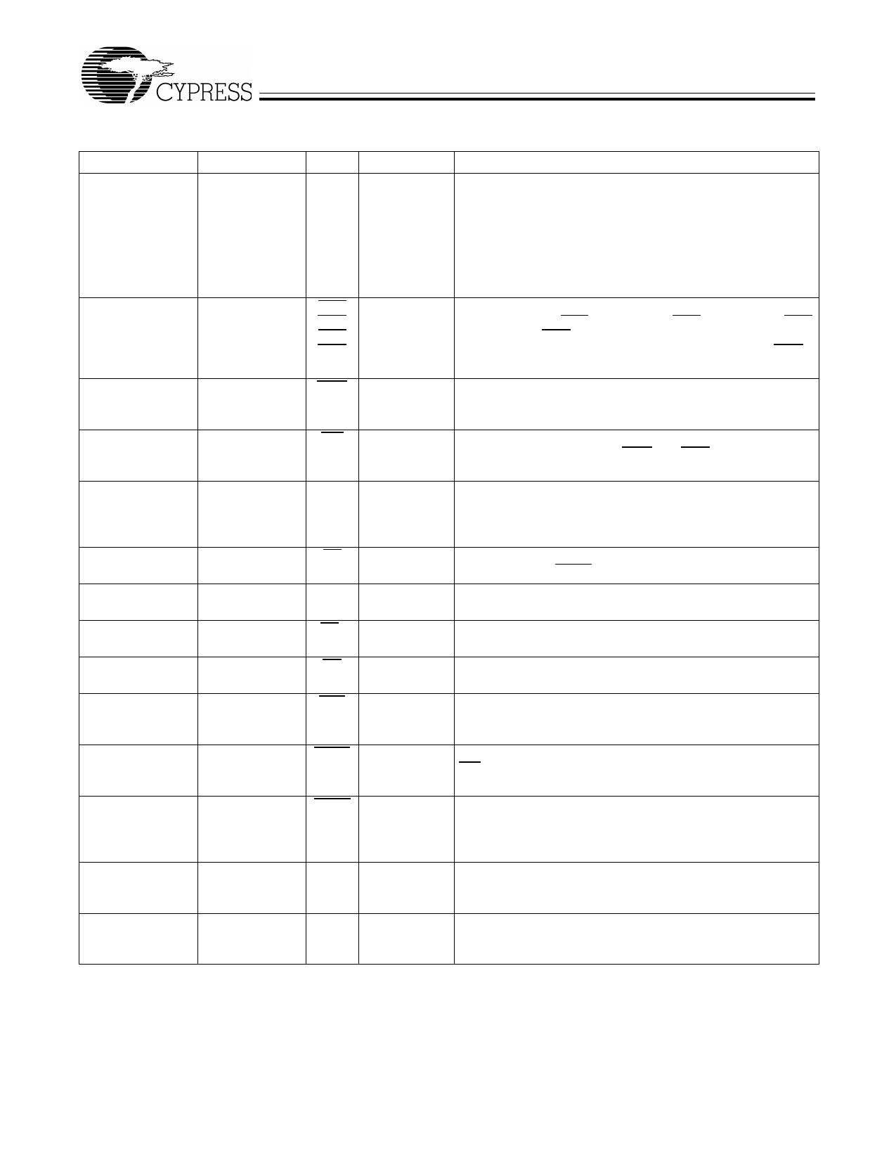
Name
A0
A1
A
BWa
BWb
BWc
BWd
BWE
GW
CLK
CE
CE2
CE2
OE
ADV
ADSP
ADSC
MODE
ZZ
Type
Description
Input-
Synchronous
Addresses: These inputs are registered and must meet the set
up and hold times around the rising edge of CLK. The burst
counter generates internal addresses associated with A0 and
A1, during burst cycle and wait cycle.
Input-
Synchronous
Byte Write: A byte write is LOW for a WRITE cycle and HIGH
for a READ cycle. BWa controls DQa. BWb controls DQb. BWc
controls DQc. BWd controls DQd. Data I/O are high imped-
ance if either of these inputs are LOW, conditioned by BWE
being LOW.
Input-
Write Enable: This active LOW input gates byte write opera-
Synchronous tions and must meet the set-up and hold times around the
rising edge of CLK.
Input-
Global Write: This active LOW input allows a full 36-bit Write
Synchronous to occur independent of the BWE and BWn lines and must
meet the set-up and hold times around the rising edge of CLK.
Input-
Synchronous
Clock: This signal registers the addresses, data, chip enables,
write control, and burst control inputs on its rising edge. All
synchronous inputs must meet set up and hold times around
the clock’s rising edge.
Input-
Chip Enable: This active LOW input is used to enable the de-
Synchronous vice and to gate ADSP.
Input-
Chip Enable: This active HIGH input is used to enable the de-
Synchronous vice.
Input-
Chip Enable: This active LOW input is used to enable the de-
Synchronous vice. Not available for B and T package versions.
Input
Output Enable: This active LOW asynchronous input enables
the data output drivers.
Input-
Address Advance: This active LOW input is used to control the
Synchronous internal burst counter. A HIGH on this pin generates wait cycle
(no address advance).
Input-
Address Status Processor: This active LOW input, along with
Synchronous CE being LOW, causes a new external address to be regis-
tered and a READ cycle is initiated using the new address.
Input-
Synchronous
Address Status Controller: This active LOW input causes de-
vice to be deselected or selected along with new external ad-
dress to be registered. A Read or Write cycle is initiated de-
pending upon write control inputs.
Input-
Static
Mode: This input selects the burst sequence. A LOW on this
pin selects Linear Burst. A NC or HIGH on this pin selects
Interleaved Burst.
Input-
Snooze: This active HIGH input puts the device in low power
Asynchronous consumption standby mode. For normal operation, this input
has to be either LOW or NC (No Connect).
5
Share Link: 