GVT71256D36T-4.4 View Datasheet(PDF) - Cypress Semiconductor
Part Name
Description
Manufacturer
GVT71256D36T-4.4 Datasheet PDF : 27 Pages
| |||
PRELIMINARY
CY7C1360A/GVT71256D36
CY7C1362A/GVT71512D18
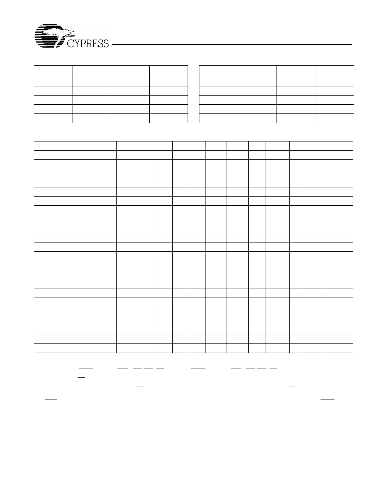
Burst Address Table (MODE = NC/VCC)
First
Address
(external)
Second
Address
(internal)
Third
Address
(internal)
Fourth
Address
(internal)
A...A00
A...A01
A...A10
A...A11
A...A01
A...A00
A...A11
A...A10
A...A10
A...A11
A...A00
A...A01
A...A11
A...A10
A...A01
A...A00
Burst Address Table (MODE = GND)
First
Address
(external)
A...A00
A...A01
A...A10
A...A11
Second
Address
(internal)
A...A01
A...A10
A...A11
A...A00
Third
Address
(internal)
A...A10
A...A11
A...A00
A...A01
Fourth
Address
(internal)
A...A11
A...A00
A...A01
A...A10
Truth Table[3, 4, 5, 6, 7, 8, 9]
Operation
Address Used CE CE2 CE2 ADSP ADSC ADV WRITE OE CLK
DQ
Deselected Cycle, Power Down None
HX X
X
L
X
X
X L-H High-Z
Deselected Cycle, Power Down None
LX L
L
X
X
X
X L-H High-Z
Deselected Cycle, Power Down None
LH X
L
X
X
X
X L-H High-Z
Deselected Cycle, Power Down None
LX L
H
L
X
X
X L-H High-Z
Deselected Cycle, Power Down None
LH X
H
L
X
X
X L-H High-Z
READ Cycle, Begin Burst
External
LL H
L
X
X
X
L L-H
Q
READ Cycle, Begin Burst
External
LL H
L
X
X
X
H L-H High-Z
WRITE Cycle, Begin Burst
External
LL H
H
L
X
L
X L-H
D
READ Cycle, Begin Burst
External
LL H
H
L
X
H
L L-H
Q
READ Cycle, Begin Burst
External
LL H
H
L
X
H
H L-H High-Z
READ Cycle, Continue Burst Next
XX X
H
H
L
H
L L-H
Q
READ Cycle, Continue Burst Next
XX X
H
H
L
H
H L-H High-Z
READ Cycle, Continue Burst Next
HX X
X
H
L
H
L L-H
Q
READ Cycle, Continue Burst Next
HX X
X
H
L
H
H L-H High-Z
WRITE Cycle, Continue Burst Next
XX X
H
H
L
L
X L-H
D
WRITE Cycle, Continue Burst Next
HX X
X
H
L
L
X L-H
D
READ Cycle, Suspend Burst Current
XX X
H
H
H
H
L L-H
Q
READ Cycle, Suspend Burst Current
XX X
H
H
H
H
H L-H High-Z
READ Cycle, Suspend Burst Current
HX X
X
H
H
H
L L-H
Q
READ Cycle, Suspend Burst Current
HX X
X
H
H
H
H L-H High-Z
WRITE Cycle, Suspend Burst Current
XX X
H
H
H
L
X L-H
D
WRITE Cycle, Suspend Burst Current
HX X
X
H
H
L
X L-H
D
Notes:
3. X = “Don’t Care.” H = logic HIGH. L = logic LOW.
For X36 product, WRITE = L means [BWE + BWa*BWb*BWc*BWd]*GW equals LOW. WRITE = H means [BWE + BWa*BWb*BWc*BWd]*GW equals HIGH.
For X18 product, WRITE = L means [BWE + BWa*BWb]*GW equals LOW. WRITE = H means [BWE + BWa*BWb]*GW equals HIGH.
4. BWa enables write to DQa. BWb enables write to DQb. BWc enables write to DQc. BWd enables write to DQd.
5. All inputs except OE must meet set up and hold times around the rising edge (LOW to HIGH) of CLK.
6. Suspending burst generates wait cycle.l
7. For a write operation following a read operation, OE must be HIGH before the input data required set-up time plus High-Z time for OE and staying HIGH throughout
the input data hold time.
8. This device contains circuitry that will ensure the outputs will be in High-Z during power-up.
9. ADSP LOW along with chip being selected always initiates a READ cycle at the L-H edge of CLK. A WRITE cycle can be performed by setting WRITE LOW for
the CLK L-H edge of the subsequent wait cycle. Refer to WRITE timing diagram for clarification.
8
Share Link: 