MPC2105C View Datasheet(PDF) - Motorola => Freescale
Part Name
Description
Manufacturer
MPC2105C
Motorola => Freescale

MPC2105C Datasheet PDF : 18 Pages
| |||
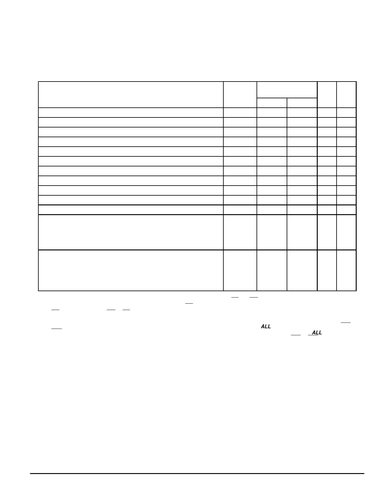
DATA RAMs AC OPERATING CONDITIONS AND CHARACTERISTICS
(VCC = 5.0 V ± 5%, VDD = 3.3 V ± 10% TA = 0 to + 70°C, Unless Otherwise Noted)
Input Timing Measurement Reference Level . . . . . . . . . . . . . . . 1.5 V
Input Pulse Levels . . . . . . . . . . . . . . . . . . . . . . . . . . . . . . . . . 0 to 3.0 V
Input Rise/Fall Time . . . . . . . . . . . . . . . . . . . . . . . . . . . . . . . . . . . . 3 ns
Output Timing Reference Level . . . . . . . . . . . . . . . . . . . . . . . . . . 1.5 V
Output Load . . . . . . . . . . . . . . See Figure 1 Unless Otherwise Noted
SYNCHRONOUS DATA RAMs READ/WRITE CYCLE TIMING (See Notes 1, 2, and 3)
MPC2105C
MPC2106C
Parameter
Symbol
Min
Max
Unit Notes
Cycle Time
tKHKH
15
—
ns
Clock Access Time
tKHQV
—
9
ns
4
Output Enable to Output Valid
tGLQV
—
5
ns
Clock High to Output Active
tKHQX1
6
—
ns
Clock High to Output Change
tKHQX2
3
—
ns
Output Enable to Output Active
tGLQX
0
—
ns
Output Disable to Q High–Z
tGHQZ
2
6
ns
Clock High to Q High–Z
tKHQZ
—
6
ns
Clock High Pulse Width
tKHKL
5
—
ns
Clock Low Pulse Width
tKLKH
5
—
ns
Setup Time
Address tAVKH
7.5
—
ns 5, 6
Setup Times:
Address Status tSVKH
2.5
Data In tDVKH
Write tWVKH
Address Advance tBAVVKH
Chip Enable tEVKH
—
ns
5
Hold Times:
Address tKHAX
0.5
Address Status tKHTSX
Data In tKHDX
Write tKHWX
Address Advance tKHBAX
Chip Enable tKHEX
—
ns
5
NOTES:
1. In setup and hold times, W (write) refers to either one or both byte write enables LW and UW.
2. All read and write cycle timings are referenced from CLK or CG.
3. CG is a don’t care when UW or LW is sampled low.
4. Maximum access times are guaranteed for all possible PowerPC external bus cycles.
5. This is a synchronous device. All addresses must meet the specified setup and hold times for ALL rising edges of CLK whenever TSP or
TSC is low, and the chip is selected. All other synchronous inputs must meet the specified setup and hold times for ALL rising edges of
CLK when the chip is enabled. Chip enable must be valid at each rising edge of clock for the device (when TSP or TSC is low) to remain
enabled.
6. 5 ns of setup delay is incurred in address buffers.
MPC2105C•MPC2106C
8
MOTOROLA FAST SRAM
Share Link: