IDT7MPV6255 View Datasheet(PDF) - Integrated Device Technology
Part Name
Description
Manufacturer
IDT7MPV6255 Datasheet PDF : 7 Pages
| |||
IDT7MPV6253/55/56
256KB/512KB CMOS SECONDARY CACHE MODULES FOR THE PowerPC
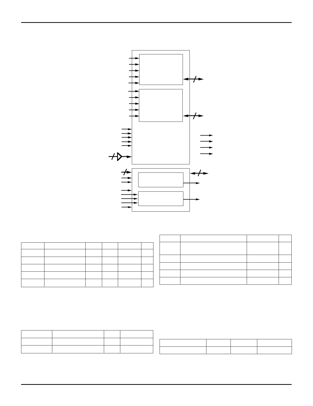
FUNCTIONAL BLOCK DIAGRAM
IDT7MPV6255 – 256KB PIPELINED BURST VERSION
COMMERCIAL TEMPERATURE RANGE
WE#0
WE#1
WE#2
WE#3
CLK1
CLK0
WE#4
WE#5
WE#6
WE#7
SRAM OE#0
SRAM ADS#0
CNT EN#0
STANDBY
BURST MODE
A14 - A28 15
32K x 32
Pipelined
Burst
SRAM
32K x 32
Pipelined
Burst
SRAM
32
DH0-31
32
DL0-31
PD0
PD1
PD2
PD3
A14 - A26 13
TWE#
TOE#
STANDBY
TCLR#
TVALID
DIRTYIN
CLK2
8K x 12
Tag Field
8K x 2
Status
12
A2 - A13
TMATCH
DIRTYOUT
drw 02
RECOMMENDED DC
OPERATING CONDITIONS
Symbol
Parameter
Min. Typ. Max. Unit
VCC3
Supply Voltage 3.14 3.3
3.6
V
VCC5
Supply Voltage 4.75 5.0
5.25
V
GND
Supply Voltage
0
0
0.0
V
VIH
Input High Voltage 2.2 — VCC + 0.3 V
VIL
Input Low Voltage –0.5(1) —
0.8
V
NOTE:
tbl 01
1. VIL = –1.0V for pulse width less than 5ns, once per cycle.
RECOMMENDED OPERATING
TEMPERATURE AND SUPPLY VOLTAGE
ABSOLUTE MAXIMUM RATINGS
Symbol
Rating
Value
Unit
VTERM Terminal Voltage with Respect –0.5 to +4.6 V
for VCC3 to GND
TA
Operating Temperature
0 to +70
°C
TBIAS Temperature Under Bias
–10 to +85 °C
TSTG Storage Temperature
–55 to +125 °C
IOUT DC Output Current
50
mA
NOTE:
tbl 03
Stresses greater than those listed under ABSOLUTE MAXIMUM RATINGS
may cause permanent damage to the device. This is a stress rating only and
functional operation of the device at these or any other conditions above those
indicated in the operational sections of this specification is not implied.
Exposure to absolute maximum rating conditions for extended periods may
affect reliability.
Power Plane Ambient Temperature GND
VCC
SRAM ACCESS TIMES
VCC3
VCC5
0°C to +70°C
0°C to +70°C
0V 3.3V +10/-5%
0V
5.0V ± 5%
Module Speed
66MHz
Asych
15ns
Burst(1)
8.5ns
Tag
10ns
tbl 02 NOTE:
tbl 04
1. Burst SRAMs are measured by Clock to Data Out (tCD).
2
Share Link: 