IDT7MPV6255 View Datasheet(PDF) - Integrated Device Technology
Part Name
Description
Manufacturer
IDT7MPV6255 Datasheet PDF : 7 Pages
| |||
IDT7MPV6253/55/56
256KB/512KB CMOS SECONDARY CACHE MODULES FOR THE PowerPC
COMMERCIAL TEMPERATURE RANGE
DC ELECTRICAL CHARACTERISTICS
(VCC5 = 5.0V ± 5%, VCC3 = 3.3V ± 10%, TA = 0°C to 70°C)
Symbol
|ILI|
|ILI|
|ILO|
VOL
VOH
ICC3
ICC5
ISB3
ISB31
Parameter
Input Leakage Current
(Address)
Input Leakage Current
(Data and Control)
Output Leakage Current
Output Low Voltage
Output HighVoltage
Operating 3.3V Power
Supply Current
Operating 5V Power
Supply Current
Standby 3.3V Power
Supply Current
Full Standby 3.3V Power
Supply Current
ISB5
Standby 5V Power
Supply Current
Test Condition
VCC5 = Max, VIN = GND to VCC
VCC3 = Max
VCC5 = Max, VIN = GND to VCC
VCC3 = Max
VOUT = 0V to VCC3, VCC3 = Max.
IOL = 8mA, VCC3 = Min.
IOH= –4mA, VCC3 = Min.
VCC3 = Max., STANDBY ≤ VIL,
f = fMAX, Outputs Open
VCC5 = Max., STANDBY ≤ VIL,
f = fMAX, Outputs Open
VCC3 = Max., STANDBY ≥ VIH,
f = fMAX, Outputs Open
VCC3 = Max., STANDBY ≥ VCC3 - 0.2V, f = 0,
VIN ≤ 0.2V or VIN ≥ VCC3 - 0.2V,
Outputs Open
VCC5 = Max., STANDBY ≥ VIH
f = fMAX, Outputs Open
Min.
—
—
—
—
2.4
—
—
—
—
—
’53
Max.
20
10
10
0.4
—
1000
290
100
30
30
’55
Max.
30
10
10
0.4
—
500
290
100
30
30
’56
Max. Unit
50 µA
20 µA
20 µA
0.4
V
—
V
590 mA
290 mA
190 mA
50 mA
30 mA
tbl 09
AC TEST CONDITIONS – 3.3V POWER SUPPLY
Input Pulse Levels
Input Rise/Fall Times
Input Timing Reference Levels
Output Reference Levels
Output Load
GND to 3.0V
3ns
1.5V
1.5V
See Figures 1 and 2
tbl 10
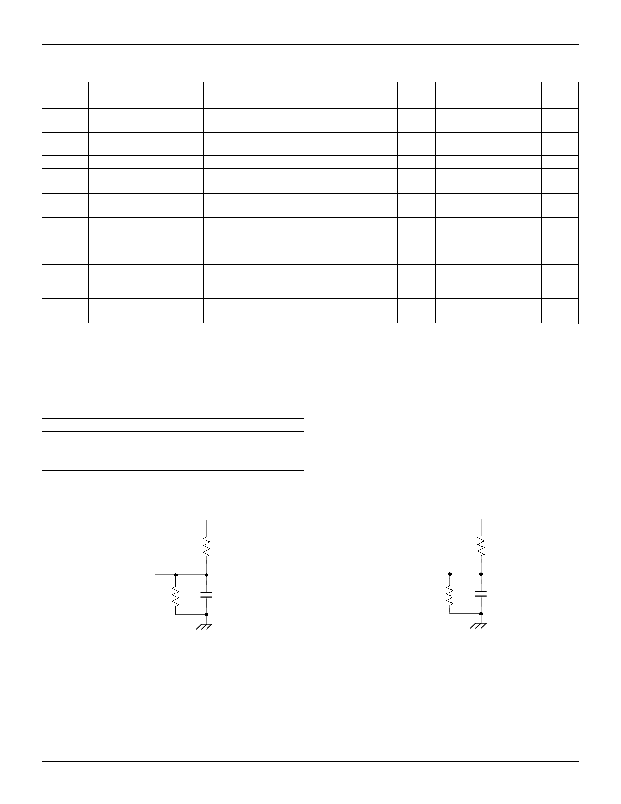
+3.3V
320Ω
DATA OUT
350Ω
30pF*
*including scope and jig capacitances
Figure 1. Output Load
drw 05
+3.3V
320Ω
DATA OUT
350Ω
5pF*
*including scope and jig capacitances
Figure 2. Output Load
(for tOHZ, tCHZ, tOLZ and tCLZ)
drw 06
5
Share Link: 