MCM32N865 View Datasheet(PDF) - Motorola => Freescale
Part Name
Description
Manufacturer
MCM32N865
Motorola => Freescale

MCM32N865 Datasheet PDF : 4 Pages
| |||
MOTOROLA
SEMICONDUCTOR TECHNICAL DATA
Advance Information
256KB Secondary Cache Module
With Tag and Optional Dirty for
486 Processor Systems
These 256K Byte cache modules offer dual asynchronous 32K x 32 banks of
memory. There is a 16K x 8 tag memory for main memory cacheability up to 64
Megabytes. The MCM32N865 and MCM32P865 include a 16K x 1 common I/O
dirty bit for writeback cache capability. The modules are designed to support
common 486 chipsets which utilize chip enable (CEx) byte control and bank write
enable (CWEx). The MCM32N864 and MCM32N865 operate at 5 V while the
MCM32P864 and MCM32P865 operate at 3.3 V power. PD pins are provided for
cache size identification at system startup
• 64MB of Cacheable Memory
• Low Profile Edge Connector: Burndy Part Number: CELP2X56SC3Z48
• All Inputs and Outputs are TTL Compatible
• Three State Outputs
• Fast Module Cycle Time: Up to External Processor Bus Speed of 33 MHz
• Cache Bank Write, Byte Chip Enable, Bank Output Enable
• Decoupling Capacitors are Used for Each Fast Static RAM
• High Quality Multi–Layer FR4 PWB With Separate Power and Ground Planes
• 5 V and 3.3 V Power Supplies are Supported
Order this document
by MCM32N864/D
MCM32N864
MCM32N865
MCM32P864
MCM32P865
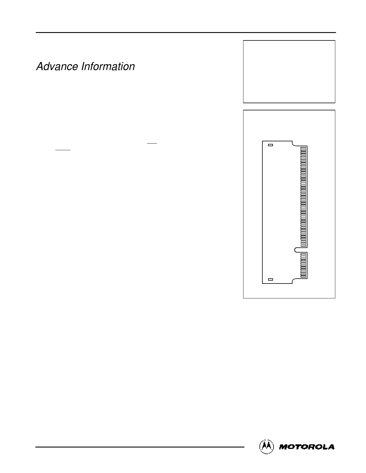
112–LEAD
CARD EDGE
CASE 1112–01
TOP VIEW
1
45
46
56
This document contains information on a new product. Specifications and information herein are subject to change without notice.
REV 1
6/95
M© OMoTtoOroRla,OInLc.A19F95AST SRAM
MCM32N864•MCM32N865•MCM32P864•MCM32P865
1
Share Link: