MPC2104PDG66 View Datasheet(PDF) - Motorola => Freescale
Part Name
Description
Manufacturer
MPC2104PDG66
Motorola => Freescale

MPC2104PDG66 Datasheet PDF : 16 Pages
| |||
TAG RAM MATCH CYCLE
Parameter
Clock High Write to MATCH Invalid
Clock High Read to MATCH Valid
Address Valid to MATCH Valid
MATCH Valid Hold from Address Change
TG Low to MATCH Invalid
TG High to MATCH Valid
TAG RAM RESET (TCLR) CYCLE
TCLR Setup Time
TCLR Hold Time
Status Bit Reset Time
Status Bit Hold from TCLR Low
TCLR Low to MATCH Invalid
TCLR High to MATCH Valid
TCLR Low to TAG High–Z
TCLR High to TAG Active
STANDBY Setup to TCLR Low
TCLR High to TWE Low
Parameter
Symbol
tKHML
tKHMV
tAVMV
tAXMX
tGLML
tGHMX
Tag RAM
Min
Max
Unit
—
7
ns
—
10
ns
—
10
ns
2
—
ns
—
7
ns
—
8
ns
Symbol
tSTC
tHTC
tSRST
tSHRS
tRSML
tRSMV
tRSQZ
tRSQX
tPDSR
tRHWX
Tag RAM
Min
Max
Unit
4
—
ns
1
—
ns
—
60
ns
2
—
ns
—
10
ns
—
100
ns
—
10
ns
—
100
ns
30
—
ns
80
—
ns
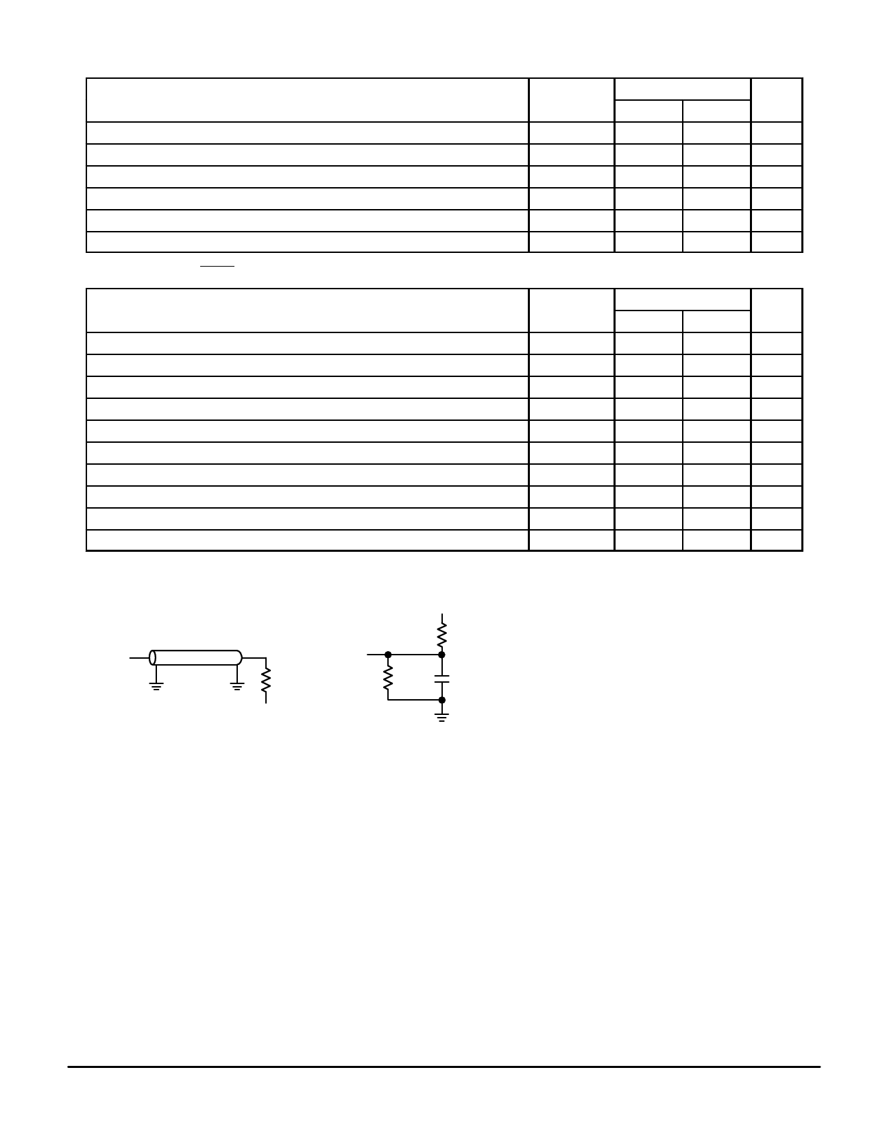
OUTPUT
Z0 = 50 Ω
OUTPUT
50 Ω
255 Ω
VL = 1.5 V
(a)
+5 V
480 Ω
5 pF
(b)
Figure 1. Test Loads
TIMING LIMITS
The table of timing values shows either a
minimum or a maximum limit for each param-
eter. Input requirements are specified from
the external system point of view. Thus, ad-
dress setup time is shown as a minimum
since the system must supply at least that
much time. On the other hand, responses
from the memory are specified from the de-
vice point of view. Thus, the access time is
shown as a maximum since the device never
provides data later than that time.
MOTOROLA FAST SRAM
MPC2104P•MPC2105P
13
Share Link: