MPC2104PDG66 View Datasheet(PDF) - Motorola => Freescale
Part Name
Description
Manufacturer
MPC2104PDG66
Motorola => Freescale

MPC2104PDG66 Datasheet PDF : 16 Pages
| |||
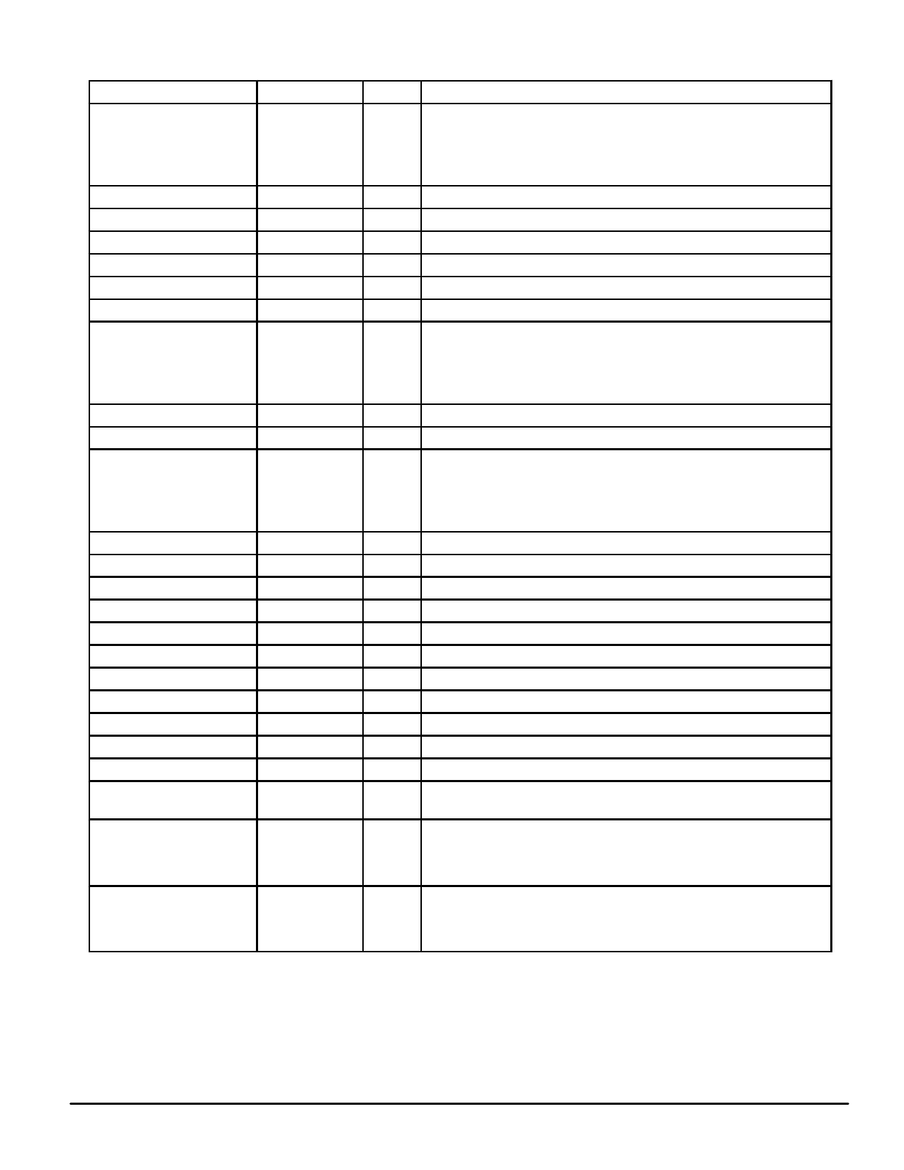
PIN DESCRIPTIONS
Pin Locations
66, 67, 68, 69, 71, 72, 73,
74, 76, 77, 78, 80, 81, 82,
83, 155, 156, 157, 158,
160, 161, 162, 163, 165,
166, 167, 169, 170, 171
64
172
59
30, 56, 115
153
138, 148
4, 5, 6, 7, 10, 11, 12, 14,
6, 17, 19, 20, 22, 24, 25,
26, 27, 93, 94, 95, 96, 99,
100, 101, 103, 105, 106,
108, 109, 111, 113, 117
88
177
32, 33, 34, 37, 38, 39, 40, 43,
44, 45, 47, 49, 50, 52, 53, 54,
119, 120, 122, 123, 124, 127,
128, 129, 131, 133, 134,
136, 137, 139, 141, 142
86
2
91
3, 92
63, 152
176
85
87
175
174
84, 173
8, 23, 51, 61, 75, 97,
112, 140, 150, 164
1, 13, 29, 31, 41, 46, 55, 57,
70, 79, 89, 90, 102, 114,
116, 121, 130, 135, 143,
145, 147, 159, 168, 178
9, 15, 18, 21, 28, 35 – 36, 42,
48, 58, 60, 62, 65, 98, 104,
107, 110, 118, 125 – 126,
132, 144, 146, 149, 151, 154
Symbol
A0 – A28
ADS0
BURSTMODE
CG0
CLK0 – CLK2
CNTEN0
CWE0 – CWE1
DH0 – DH31
DIRTYIN
DIRTYOUT
DL0 – DL31
MATCH
PD0/IDSCLK
PD1/IDSDATA
PD2, PD3
RESERVED
STANDBY
TCLR
TG
TWE
VALIDIN
VCC
VDD
VSS
NC
Type
Input
Description
Address Inputs — (MSB:0, LSB:28).
Input
Input
Input
Input
Input
Input
I/O
Data RAM Address Strobe.
Burstmode. 0 = Linear, 1 = Interleaved.
Data RAM Output Enable.
Clock Inputs — CLK2 is for Tag RAM, CLK0 and CLK1 are for Data RAMs only.
Data RAM Count Enable.
Data RAM Write Enables — (MSB:0, LSB:1).
High Data Bus — (MSB:0, LSB:31).
Input
Output
I/O
Dirty input bit.
Dirty output bit.
Low Data Bus — (MSB:0, LSB:31).
Output
Input
I/O
Output
Input
Input
Input
Input
Input
Input
Input
Tag RAM active high match indication.
Presence detect bit 0/EEPROM serial clock. (EEPROM option only).
Presence detect bit 1/EEPROM serial data. (EEPROM option only).
Presence detect bits.
Reserved pin.
Standby pin. Reduces standby power consumption.
Tag RAM clear.
Tag RAM output enable.
Tag RAM write enable.
Tag RAM valid bit.
+ 5 V power supply. Must be connected.
+ 3.3 V power supply. Must be connected.
Input Ground.
— There is no connection to the module.
MOTOROLA FAST SRAM
MPC2104P•MPC2105P
5
Share Link: