MPC2104PDG66 View Datasheet(PDF) - Motorola => Freescale
Part Name
Description
Manufacturer
MPC2104PDG66
Motorola => Freescale

MPC2104PDG66 Datasheet PDF : 16 Pages
| |||
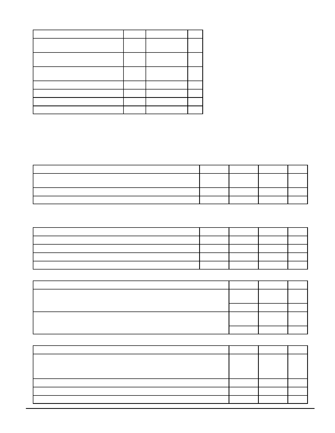
ABSOLUTE MAXIMUM RATINGS (Voltages Referenced to VSS = 0 V)
Rating
Symbol
Value
Unit
Power Supply Voltage
Tag VCC
– 0.5 to + 7.0
V
Data RAM VDD
– 0.5 to + 4.6
Voltage Relative to VSS
Tag Vin, Vout – 0.5 to VCC + 0.5 V
Data RAM
– 0.5 to VDD + 0.5
Output Current (per I/O)
Tag Iout
Data RAM
± 20
mA
± 30
Power Dissipation
PD
3.86
W
Temperature Under Bias
Tbias
– 10 to + 85
°C
Operating Temperature
TA
0 to +70
°C
Storage Temperature
Tstg
– 55 to + 125
°C
NOTE: Permanent device damage may occur if ABSOLUTE MAXIMUM RATINGS are
exceeded. Functional operation should be restricted to RECOMMENDED OPER-
ATING CONDITIONS. Exposure to higher than recommended voltages for
extended periods of time could affect device reliability.
This device contains circuitry to protect the
inputs against damage due to high static volt-
ages or electric fields; however, it is advised
that normal precautions be taken to avoid
application of any voltage higher than maxi-
mum rated voltages to this high–impedance
circuit.
This BiCMOS memory circuit has been
designed to meet the dc and ac specifications
shown in the tables, after thermal equilibrium
has been established.
This device contains circuitry that will ensure
the output devices are in High–Z at power up.
DC OPERATING CONDITIONS AND CHARACTERISTICS
(VCC = 5.0 V ± 5%, VDD = 3.3 V + 10%, – 5%, TA = 0 to + 70°C, Unless Otherwise Noted)
RECOMMENDED OPERATING CONDITIONS (Voltages Referenced to VSS = 0 V)
Parameter
Symbol
Min
Max
Unit
Supply Voltage (Operating Voltage Range)
VCC
VDD
Input High Voltage
VIH
Input Low Voltage
VIL
* VIL (min) = – 0.5 V dc; VIL (min) = – 2.0 V ac (pulse width ≤ 20 ns) for I ≤ 20.0 mA.
** VIH (max) = VDD + 0.3 V dc; VIH (max) = VDD + 2.0 V ac (pulse width ≤ 20 ns) for I ≤ 20.0 mA.
4.75
3.135
2.2
– 0.5*
5.25
V
3.60
VDD + 0.3**
V
0.8
V
DC CHARACTERISTICS
Parameter
Input Leakage Current (All Inputs, Vin = 0 to VDD)
Output Leakage Current (CG = VIH, Vout = 0 to VDD)
TTL Output Low Voltage (IOL = + 8.0 mA)
TTL Output High Voltage (IOH = – 4.0 mA)
Symbol
Min
Ilkg(I)
—
Ilkg(O)
—
VOL
—
VOH
2.4
Max
Unit
± 1.0
µA
± 1.0
µA
0.4
V
—
V
POWER SUPPLY CURRENTS
Parameter
Symbol
Max
Unit
AC Supply Current (CG = VIH, E = VIL, Iout = 0 mA, All Inputs = VIL and VIH,
VIL = 0.0 V and VIH ≥ 3.0 V, Cycle Time ≥ 20 ns)
MPC2104P
MPC2105P
IDDA
410
mA
700
ICCA
320
mA
AC Standby Current (E = VIH, Iout = 0 mA, All Inputs = VIL or VIH
VIL = 0.0 V and VIH ≥ 3.0 V, Cycle Time ≥ 20 ns)
MPC2104P ISB1 (VDD)
210
mA
MPC2105P
240
ISB1 (VCC)
320
mA
CAPACITANCE (f = 1.0 MHz, dV = 3.0 V, TA = 25°C, Periodically Sampled Rather Than 100% Tested)
Parameter
Symbol
Input Capacitance
(A13 – A28)
Cin
(Data RAM Control Pins)
(CLK0 – CLK2)
(Tag Control Pins)
Tag Output Capacitance
Data RAM Input/Output Capacitance
Tag Input/Output Capacitance
(MATCH, DIRTYOUT)
(DH0 – DH31, DL0 – DL31)
(A0 – A11)
Cout
CI/O
CI/O
Max
Unit
15
pF
10
5
5
7
pF
8
pF
7
pF
MOTOROLA FAST SRAM
MPC2104P•MPC2105P
7
Share Link: