AN5693 View Datasheet(PDF) - Panasonic Corporation
Part Name
Description
Manufacturer
AN5693
Panasonic Corporation

AN5693 Datasheet PDF : 34 Pages
| |||
ICs for TV
AN5693K
s Pin Equivalent Circuit(continued)
Pin No.
Equivalent Circuit
Function
Status
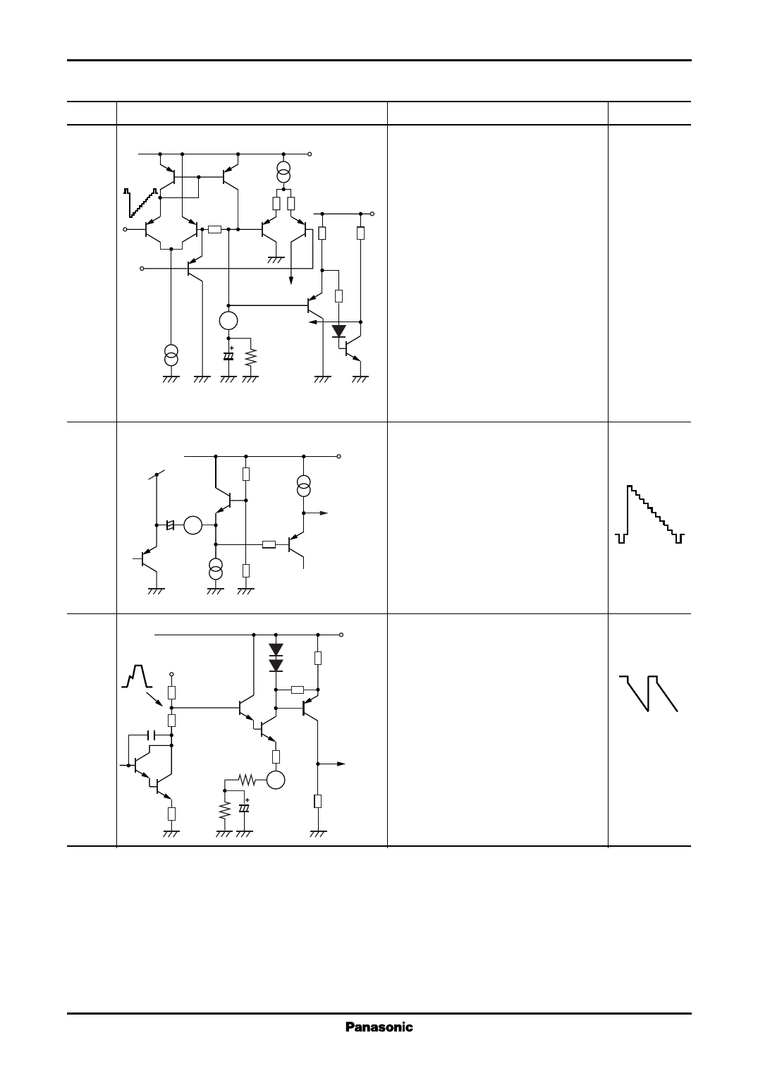
30
−Y
5.1 V
100 µA
80 µA
10 kΩ
9V
(VCC1)
5V
(VCC3)
80 kΩ
Black level detecion output pin blanking
off switch pin :
• For black expansion circuit's black
level detection output filter pin
• For removing the blanking period and
DC
abuot 5.1 V
To black
expansion
circuit
30
To
blanking
circuit
180 kΩ
R
4.7 µF
75 kΩ
10 kΩ
holding the darkest Y level
• By changing the external resistor, R,
the black level expansion sensitivity
can be changed. When R is bigger, area
of response is smaller
• To stop black expansion circuit, set
Pin30 voltage to about VCC(9 V)
• If Pin30 voltage is GND, blanking is
off.(Black expansion is also off)
31
Video Input Pin :
AC
47 kΩ
4.3 V
9V
(VCC1)
50 µA
• Video signal input pin
(Composite video also allowable)
• Standard input 0.6 VPP
0.6 VPP
31
1.8 kΩ
• Sync. top is clamped to 3.5 V
• Video signal is inputed to low impedance
10 µA
43 kΩ
inputs
32
5 V Vertical Synchronous Signal Clamp Pin :
AC
4.3 V
16 kΩ
(VCC3)
3 kΩ
50 kΩ
• This is the peak clamp pin for vertical
synchronous signal separation
• The integration of the vertical
f = fV
200 Ω
4 kΩ
R1
680 kΩ
To ver.
R2
220 Ω
270 Ω count down
32
C1
2.2 µF
synchronous signal is determined by
the internal time constant, but the
external time constant, R1, C1, is chosen
according to the required trigger timing
• Using R1 > 200 kΩ
• R2 is the resistor which is used to
control the emitter current
21
Share Link: