AP7365 View Datasheet(PDF) - Diodes Incorporated.
Part Name
Description
Manufacturer
AP7365 Datasheet PDF : 20 Pages
| |||
AP7365
600mA, Low Quiescent Current, Fast Transient
Low Dropout Linear Regulator
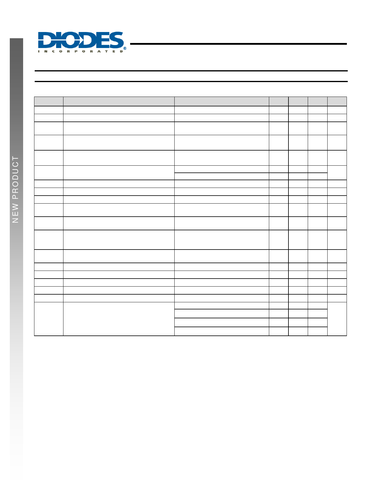
Electrical Characteristics
(TA = 25oC, VIN = VOUT +1V, CIN = 1μF, COUT = 1μF, VEN = 2V, unless otherwise stated)
Symbol
Parameter
Test Conditions
Min Typ. Max Unit
VREF ADJ Reference Voltage (Adjustable version) IOUT= 0mA
IADJ ADJ Leakage (Adjustable version)
VOUT Output Voltage Accuracy
TA = -40oC to 85oC,
IOUT = 10% of IOUT-Max
-2
ΔVOUT Line Regulation
/ΔVIN/V
VIN = (VOUT +1V) to VIN-Max,
VEN = VIN, IOUT = 1mA
ΔVOUT Load Regulation
/VOUT
VIN = (VOUT +1V) to VIN-Max,
IOUT = 1mA to 600mA
-1.0
VDropout Dropout Voltage (Note 3)
VOUT < 2.5V, IOUT = 600mA
VOUT ≥ 2.5V, IOUT = 600mA
IQ Input Quiescent Current
VEN = VIN, IOUT = 0mA
ISHDN Input Shutdown Current
VEN = 0V, IOUT = 0mA
ILEAK Input Leakage Current
VEN = 0V, OUT grounded
tST Start-up Time
VEN = 0V to 2.0V in 1μs,
IOUT = 600mA
PSRR PSRR (Note 4)
VIN = [VOUT +1V]VDC + 0.5VppAC,
f = 1kHz, IOUT = 50mA
ISHORT Short-circuit Current
VIN = VIN-Min to VIN-Max,
VOUT < 0.2V (fixed version) or 25% of
VOUT (ADJ version)
ILIMIT Current limit
VIN = VIN-Min to VIN-Max,
VOUT/ROUT = 2.5A
0.8
VIL EN Input Logic Low Voltage
VIN = VIN-Min to VIN-Max
VIH EN Input Logic High Voltage
VIN = VIN-Min to VIN-Max
1.4
IEN EN Input Current
VIN = 0V or VIN-Max
-1
TSHDN Thermal shutdown threshold
THYS Thermal shutdown hysteresis
SOT25 (Note 5)
DFN2020-6 (Note 5)
θJA Thermal Resistance Junction-to-Ambient SOT89-3L (Note 5)
0.8
0.1
0.02
370
300
35
0.1
0.1
200
65
240
1.4
145
15
187
251
141
V
1
μA
2
%
0.20 %/V
1.0 %
600
400
mV
80 μA
1
μA
1
μA
μs
dB
mA
A
0.4 V
V
1
μA
°C
°C
oC/W
SOT223-3L (Note 5)
153
Notes:
3. Dropout voltage is the voltage difference between the input and the output at which the output voltage drops 2% below its nominal
value. This parameter only applies to input voltages above minimum VIN = 2.0V.
4. At VIN < 2.3V, the PSRR performance may be reduced.
5. Test condition for all packages: Device mounted on FR-4 substrate PC board, 1oz copper, with minimum recommended pad
layout.
AP7365
Document number: DS32260 Rev. 2 - 2
4 of 20
www.diodes.com
September 2010
© Diodes Incorporated
Share Link: 