APA2180 View Datasheet(PDF) - Anpec Electronics
Part Name
Description
Manufacturer
APA2180 Datasheet PDF : 22 Pages
| |||
APA2180
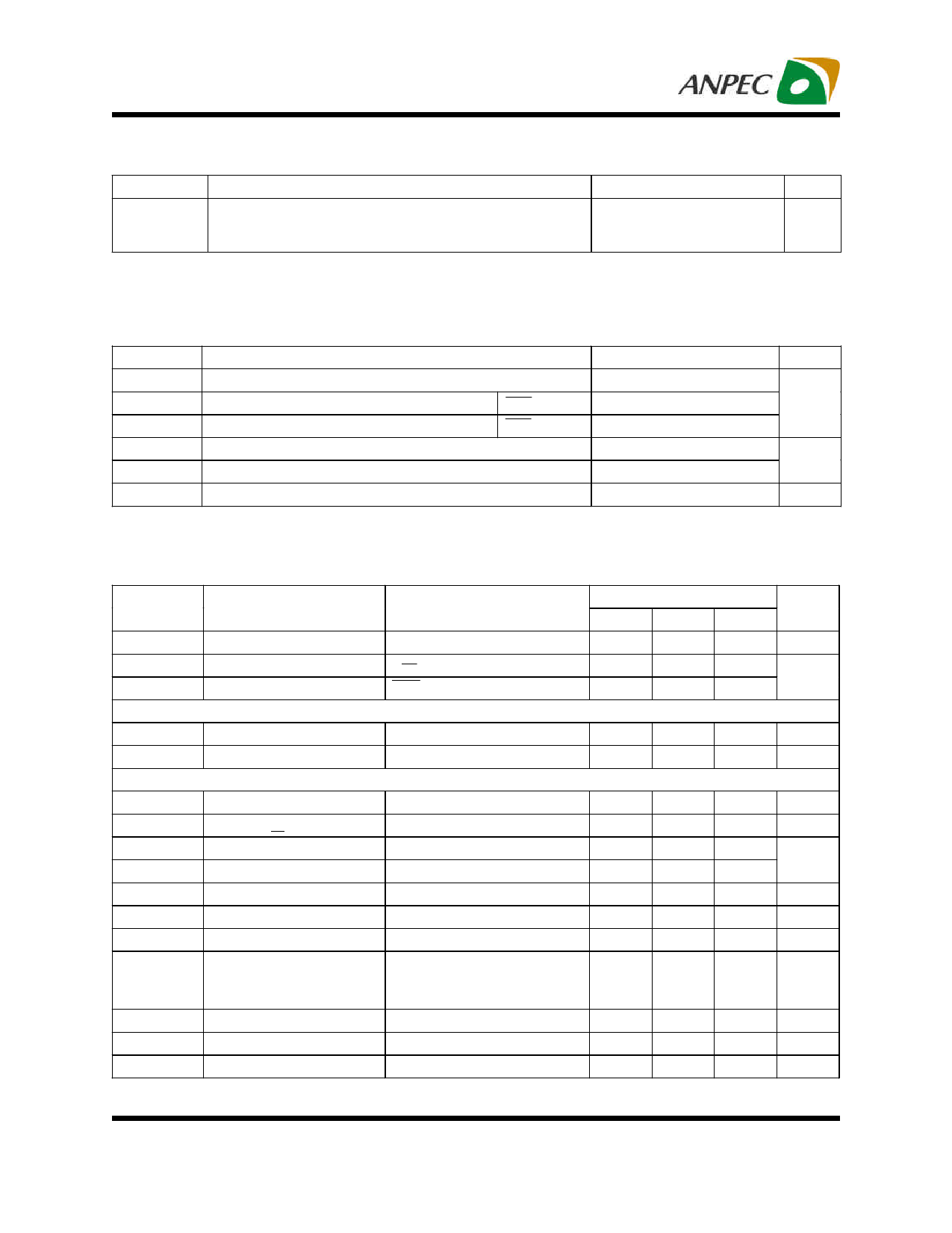
Thermal Characteristics
Symbol
θJA
Parameter
Thermal Resistance - Junction to Ambient (Note 2)
WLCSP1.6x1.6-12
TDFN3x3-12
Typical Value
160
50
Unit
OC/W
Note 2: Please refer to “Thermal Pad Consideration”. 2 layered 5 in2 printed circuit boards with 2oz trace and copper through several
thermal vias. The thermal pad is soldered on the PCB.
Recommended Operating Conditions
Symbol
VDD
VIH
VIL
TA
TJ
RL
Supply Voltage
Parameter
High Level Threshold Voltage
Low Level Threshold Voltage
Operating Ambient Temperature Range
Operating Ambient Temperature Range
Headphone Resistance
SDN
SDN
Range
2.3 ~ 5.5
1.0 ~ VDD
0 ~ 0.35
-40 ~ 85
-40 ~ 125
16 ~ 100k
Unit
V
ΟC
Ω
Electrical Characteristics
VDD=3.6V, VGND=VPGND=0V, VSDN=VDD, CCPF=CCPO=1µF, Ci=1µF, TA=25oC (unless otherwise noted).
Symbol
Parameter
Test Conditions
Min.
APA2180
Typ.
IDD
VDD Supply Current
ISD
VDD Shutdown Current
II
Input current
CHARGE PUMP
VSDN=0V
SDN
-
1
-
5
-
0.1
fOSC
Req
DRIVERS
Switching Frequency
Equivalent Resistance
400
500
-
15
AV
Internal Voltage Gain
No Load
-1.55
-1.5
△AV
Gain Matching
-
1
Ri
Input Resistance
12
14
Rf
Feedback Resistance
17
21
VSR
Slew Rate
-
2.5
VOS
Output Offset Voltage
VDD=2.3V to 5.5V, RL = 16Ω
-8
-
VN
Output Noise
-
27
VDD=2.3V to 5.5V, Vrr=200mVrms
PSRR
Power Supply Rejection Ratio
fin= 217Hz
fin= 1kHz
-
-80
-80
fin= 20kHz
-40
CL
Maximum Capacitive Load
-
400
Tstart-up
Start-up Time
-
4
VESD
ESD Protection
OUTR, OUTL
-
8
Max.
2
10
-
600
18
-1.45
2
16
25
-
8
-
-60
-60
-35
-
-
-
Unit
mA
µA
kHz
Ω
V/V
%
kΩ
V/µs
mV
µVrms
dB
pF
ms
kV
Copyright © ANPEC Electronics Corp.
4
Rev. A.3 - Dec., 2012
www.anpec.com.tw
Share Link: 