APL1187 View Datasheet(PDF) - Anpec Electronics
Part Name
Description
Manufacturer
APL1187 Datasheet PDF : 9 Pages
| |||
APL1187
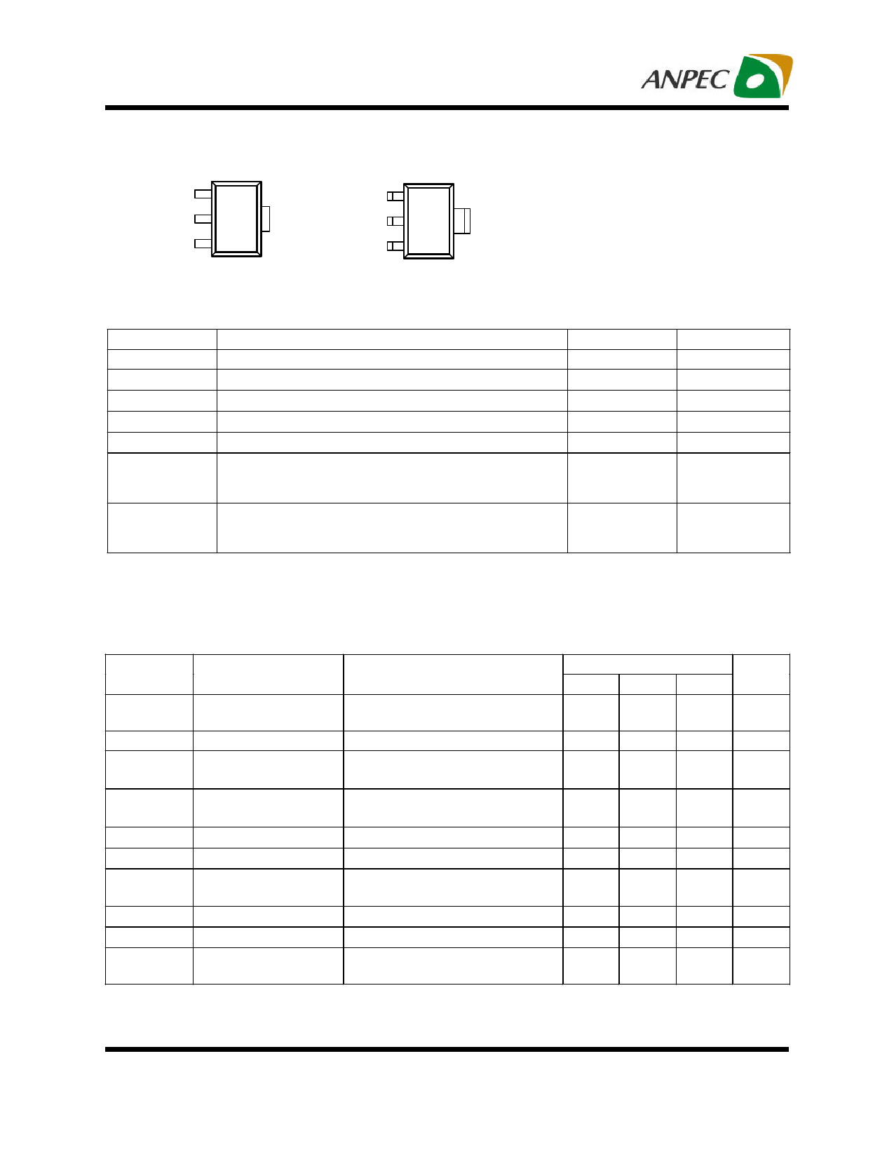
Pin Configurations
SOT-89 Top View
VOUT 1
GND 2
VIN 3
GND
(Tab)
APL1187
SOT-223 Top View
VOUT 1
GND 2
VIN 3
GND
(Tab)
APL1187
Absolute Maximum Ratings (Note 1,2)
Symbol
Parameter
Rating
Unit
VI
Input Voltage
9
V
PD
Power Dissipation, TA=25°C
1.3
W
TJ
Operating Junction Temperature Range
0 to 150
°C
TSTG
Storage Temperature Range
-65 to +150
°C
TL
Lead Temperature (Soldering, 10 second)
260
°C
Thermal Resistance from Junction to Ambient
θJA
SOT-89
SOT-223
Thermal Resistance from Junction to Case
θJC
SOT-89
SOT-223
130
75
°C/W
40
15
°C/W
Note 1: Stresses beyond the absolute maximum rating may damage the device and operating in the absolute maximum rating conditions may affect
device reliability.
Note 2: The maximum allowable power dissipation at any TA (ambient temperature) is calculated using: PD (max) = (TJ – TA) / θJA; TJ = 125°C. Exceeding
the maximum allowable power dissipation will result in excessive die temperature.
Electrical Characteristics
Symbol
Parameter
Test Conditions
APL1187
Unit
Min
Typ
Max
VOUT
Output Voltage
APL1187-12
TJ =0~125°C, 0≤ IOUT≤ 0.6A,
2.8V≤VIN≤9V,
1.176 1.200 1.224
V
VIN
REGLINE
REGLOAD
VD
ILIMIT
PSRR
Input Voltage
Line Regulation
APL1087-12
Load Regulation
APL1187-12
Dropout Voltage
Current Limit
Ripple Rejection
TJ =0~125°C, IOUT=0mA,
2.8V≤VIN≤9V (note3)
TJ =0~125°C, VIN=2.8V,
0≤ IOUT ≤0.6A (note 3)
IOUT=0.6A, TJ =0~125°C
(VIN -VOUT)=5V, TJ=25°C
FRIPPLE=120Hz, VRIPPLE=1VP-P,
(VIN -VOUT)=3V, TJ=0~125°C
2.8
9
V
1
6
mV
0.4
0.6
%
1.4
1.55
V
800
mA
60
75
dB
OT
Over Temperature Point
150
°C
OTP Hysteresis
20
°C
Quiescent Current
IQ
APL1187-12
TJ=0~125°C, VIN≤9V
5.5
10
mA
Note 3: See thermal regulation specifications for changes in output voltage due to heating effects. Load line regulations are measured at a constant junction
temperature by low duty cycle pulse testing.
Note 4: Dropout voltage is specified over the full output current range of the device. Dropout voltage is defined as the minimum input/output differential
measured at the specified output current. Test points and limits are also shown on the Dropout Voltage curve.
Copyright © ANPEC Electronics Corp.
2
Rev. A.2 - Nov., 2006
www.anpec.com.tw
Share Link: 