APU3137 View Datasheet(PDF) - Advanced Power Electronics Corp
Part Name
Description
Manufacturer
APU3137 Datasheet PDF : 17 Pages
| |||
APU3137
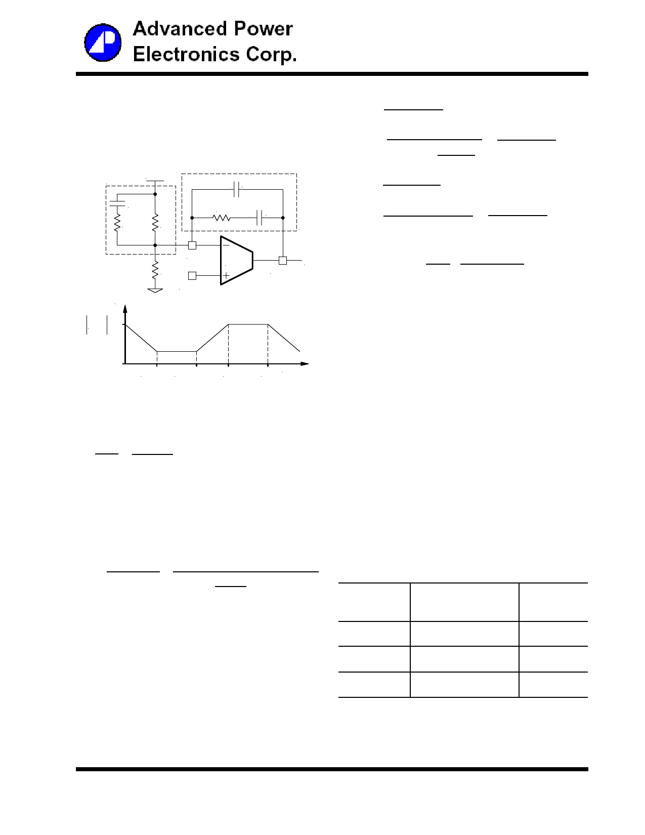
For a general solution for unconditionally stability for
ceramic capacitor with very low ESR and any type of
output capacitors, in a wide range of ESR values we
should implement local feedback with a compensation
network. The typically used compensation network for
voltage-mode controller is shown in Figure 10.
ZIN
VOUT
C10
R8
R6
C12
R7
C11
Zf
Gain(dB)
H(s) dB
Fb E/A
R5
Vp=VREF
Ve
Comp
FP1 = 0
FP2 =
1
2π×R8×C10
( ) FP3 =
1
2π×R7×
C12×C11
C12+C11
≅
1
2π×R7×C12
FZ1 =
1
2π×R7×C11
1
1
FZ2 = 2π×C10×(R6 + R8) ≅ 2π×C10×R6
Cross Over Frequency:
FO
=
R7×C10×
VVOISNC×
1
2π×Lo×Co
Where:
VIN = Maximum Input Voltage
VOSC = Oscillator Ramp Voltage
Lo = Output Inductor
Co = Total Output Capacitors
---(21)
FZ1 FZ2
FP2
FP3 Frequency
Figure 10 - Compensation network with local
feedback and its asymptotic gain plot.
The stability requirement will be satisfied by placing the
poles and zeros of the compensation network according
to following design rules. The consideration has been
taken to satisfy condition (20) regarding transconduc-
tance error amplifier.
In such configuration, the transfer function is given by:
Ve
VOUT
=
1 - gmZf
1 + gmZIN
The error amplifier gain is independent of the transcon-
ductance under the following condition:
gmZf >> 1 and gmZIN >>1
---(20)
These design rules will give a crossover frequency ap-
proximately one-tenth of the switching frequency. The
higher the band width, the potentially faster the load tran-
sient speed. The gain margin will be large enough to
provide high DC-regulation accuracy (typically -5dB to -
12dB). The phase margin should be greater than 45 for
overall stability.
By replacing ZIN and Zf according to Figure 7, the trans-
former function can be expressed as:
[ ( )] H(s)
=
1
sR6(C12+C11)
×
(1+sR7C11)×[1+sC10(R6+R8)]
C12C11
1+sR7 C12+C11 ×(1+sR8C10)
As known, transconductance amplifier has high imped-
ance (current source) output, therefore, consider should
be taken when loading the E/A output. It may exceed its
source/sink output current capability, so that the ampli-
fier will not be able to swing its output voltage over the
necessary range.
The compensation network has three poles and two ze-
ros and they are expressed as follows:
Based on the frequency of the zero generated by ESR
versus crossover frequency, the compensation type can
be different. The table below shows the compensation
type and location of crossover frequency.
Compensator Location of Zero
Type Crossover Frequency
(FO)
Type II (PI)
FPO < FZO < FO < fS/2
Type III (PID)
Method A
Type III (PID)
Method B
FPO < FO < FZO < fS/2
FPO < FO < fS/2 < FZO
Typical
Output
Capacitor
Electrolytic,
Tantalum
Tantalum,
Ceramic
Ceramic
Table - The compensation type and location of zero
crossover frequency.
Detail information is dicussed in application Note AN-
1043 which can be downloaded from the IR Web-Site.
11/17
Share Link: 