5962-9669201HTA View Datasheet(PDF) - Austin Semiconductor
Part Name
Description
Manufacturer
5962-9669201HTA Datasheet PDF : 27 Pages
| |||
Austin Semiconductor, Inc.
FLASH
AS29F040
WRITE OPERATION STATUS
DQ6: Toggle Bit I
The device provides several bits to determine the status of
Toggle bit I on DQ6 indicates whether an Embedded
a write operation: DQ2, DQ3, DQ5, DQ6, and DQ7. Table 5 and Program or Erase algorithm is in progress or complete, or whether
the following subsections describe the functions of these bits. the device has entered the Erase Suspend mode. Toggle Bit I
DQ7 and DQ6 each offer a method for determining whether a may be read at any address, and is valid after the rising edge of
program or erase operation is complete or in progress. These the final WE\ pulse in the command sequence (prior to the
three bits are discussed first.
program or erase operation), and during the sector erase time-
out.
DQ7: Data\ Polling
During an Embedded Program or Erase algorithm
The Data\ Polling bit, DQ7, indicates to the host system operation, successive read cycles to any address cause DQ6 to
whether an Embedded Algorithm is in progress or completed,
or whether the device is in Erase Suspend. Data\ Polling is
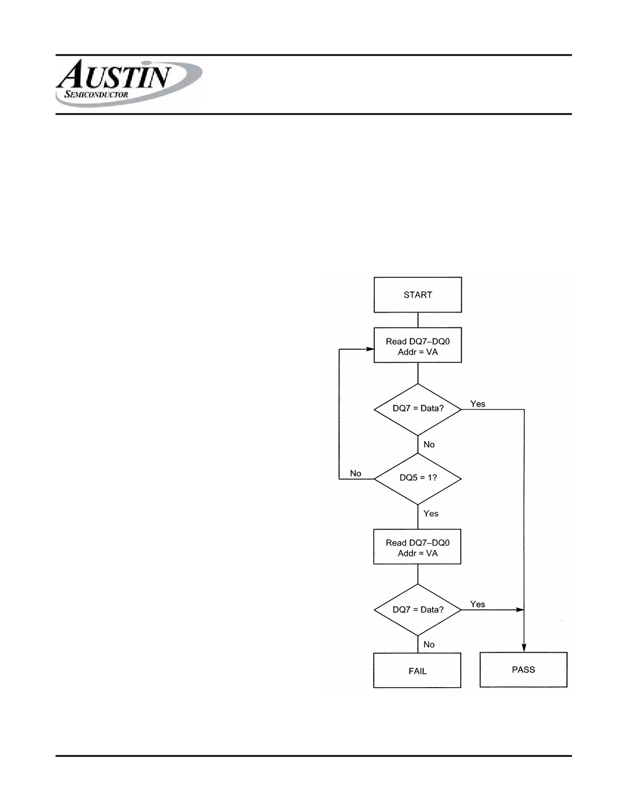
FIGURE 3: DATA\ POLLING ALGORITHM
valid after the rising edge of the final WE\ pulse in the program
or erase command sequence.
During the Embedded Program algorithm, the device
outputs on DQ7 the complement of the datum programmed to
DQ7. This DQ7 status also applies to programming during
Erase Suspend. When the Embedded Program algorithm is
complete, the device outputs the datum programmed to DQ7.
The system must provide the program address to read valid
status information on DQ7. If a program address falls within a
protected sector, Data\ Polling on DQ7 is active for
approximately 2µs, then the device returns to reading array
data.
During the Embedded Erase algorithm, Data\ Polling
produces a “0” on DQ7. When the Embedded Erase algorithm
is complete, or if the device enters the Erase Suspend mode,
Data\ Polling produces a “1” on DQ7. This is analogous to the
complement/true datum output described for the Embedded
Program algorithm: the erase function changes all the bits in a
sector to “1”; prior to this, the device outputs the
“complement,” or “0”. The system must provide an address
within any of the sectors selected for erasure to read valid
status information on DQ7.
After an erase command sequence is written, if all sectors
selected for erasing are protected, Data\ Polling on DQ7 is
active for approximately 100µs, then the device returns to
reading array data. If not all selected sectors are protected, the
Embedded Erase algorithm erases the unprotected sectors, and
ignores the selected sectors that are protected.
When the system detects DQ7 has changed from the
complement to true data, it can read valid data at DQ7-DQ0 on
the following read cycles. This is because DQ7 may change
asynchronously with DQ0-DQ6 while Output Enable (OE\) is
asserted low. The Data\ Polling Timings (During Embedded
Algorithms) figure in the “AC Characteristics” section
illustrates this.
Table 5 shows the outputs for Data\ Polling on DQ7.
Figure 3 shows the Data\ Polling algorithm.
NOTE:
1) VA = Valid address for programming. During a sector erase operation,
a valid address is an address within any sector selected for erasure. During
chip erase, a valid address is any non-protected sector address.
2) DQ7 should be rechecked even if DQ5 = “1” because DQ7 may change
simultaneously with DQ5.
AS29F040
Rev. 2.2 09/07
10
Austin Semiconductor, Inc. reserves the right to change products or specifications without notice.
Share Link: 