AS3931 View Datasheet(PDF) - austriamicrosystems AG
Part Name
Description
Manufacturer
AS3931 Datasheet PDF : 31 Pages
| |||
AS3931
Datasheet - Electrical Characteristics
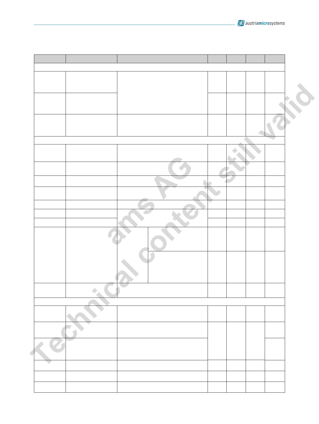
Table 3. Electrical Characteristics
Symbol
WAKEUP
Parameter
Conditions
Min Typ Max Units
minimum differential input
Vin,min
voltage for wake up
detection10
350
NPRE = 8
trise,tfall < 150 µs;
Vin,max
maximum differential input
voltadgeetefcotriowna1k0e up
VREG = 2.4 V to 3.5 V11
1
Voltage at WAKE pin:
IWAKE
WAKE pin current
VOL < 0.4 V;
0.33
VREG = 2.4 V to 3.5 V11
RSSI
ill VRSSI
RSSI output voltage range
0.5
1.7
t VRSSI0
RSSI output voltage
(RSSI offset)
VIN = 0;
0.5
0.76
1.2
G VSTEP
RSSI output voltage step12
VIN = 1 mVpp;
100 290
A t s VLOG
logarithmic input voltage
range
VIN = 1 mVpp, RSSI step = high
0.3
300
SRSSI
RSSI slope in log. range
RSSI step = high
12
s n CRSSI
cap. loading of RSSI pin
10
RSSI buffer active
e IRSSI
RSSI buffer output current
5
m t Input signal amplitude
100 mVpp; CS from low to high
a n (Buffer activation in presence of
350
a strong input signal);
o Tstep
RSSI voltage step time13
CL = 10 pF,
RL = 1 MΩ;
channel switching from ChA(100
mVpp) to
c ChB (0 mVpp)14,
350
with CS deactivation of
l 10 µs
a VRIP
RSSI Ripple Voltage
RSSI buffer active, CL = 10 pF, RL = 1 MΩ;
VIN = 1 mVpp;
70
ic Serial Programming Interface
n VIL
Digital input L level
Pins SCL, SDA, CS;
VREG = 2.4 V to 3.5 V11
0.3 *
VREG11
h VIH
Digital input H level
Pins SCL, SDA, CS
VREG = 2.4 V to 3.5 V11
0.7 *
VREG11
ec IIH
Digital Input current
Pins SCL, SDA, CS
VIH = 2.4 V;
VREG = 2.4 V to 3.5 V11
30
60
100
TTCLK
Clock period
VREG = 2.4 V to 3.5 V11
2
µVpp
valid Vpp
mA
V
V
mV
mV
mV/dB
pF
µA
µs
µs
mV
V
V
µA
µs
TCH
Clock high duration
VREG = 2.4 V to 3.5 V11
500
ns
TCL
Clock low duration
VREG = 2.4 V to 3.5 V11
500
ns
www.austriamicrosystems.com
Revision 6.2
7 - 30
Share Link: 