AT25F512B View Datasheet(PDF) - Atmel Corporation
Part Name
Description
Manufacturer
AT25F512B Datasheet PDF : 34 Pages
| |||
AT25F512B [Preliminary]
5. Device Operation
The AT25F512B is controlled by a set of instructions that are sent from a host controller, com-
monly referred to as the SPI Master. The SPI Master communicates with the AT25F512B via the
SPI bus which is comprised of four signal lines: Chip Select (CS), Serial Clock (SCK), Serial
Input (SI), and Serial Output (SO).
The SPI protocol defines a total of four modes of operation (mode 0, 1, 2, or 3) with each mode
differing in respect to the SCK polarity and phase and how the polarity and phase control the
flow of data on the SPI bus. The AT25F512B supports the two most common modes, SPI Modes
0 and 3. The only difference between SPI Modes 0 and 3 is the polarity of the SCK signal when
in the inactive state (when the SPI Master is in standby mode and not transferring any data).
With SPI Modes 0 and 3, data is always latched in on the rising edge of SCK and always output
on the falling edge of SCK.
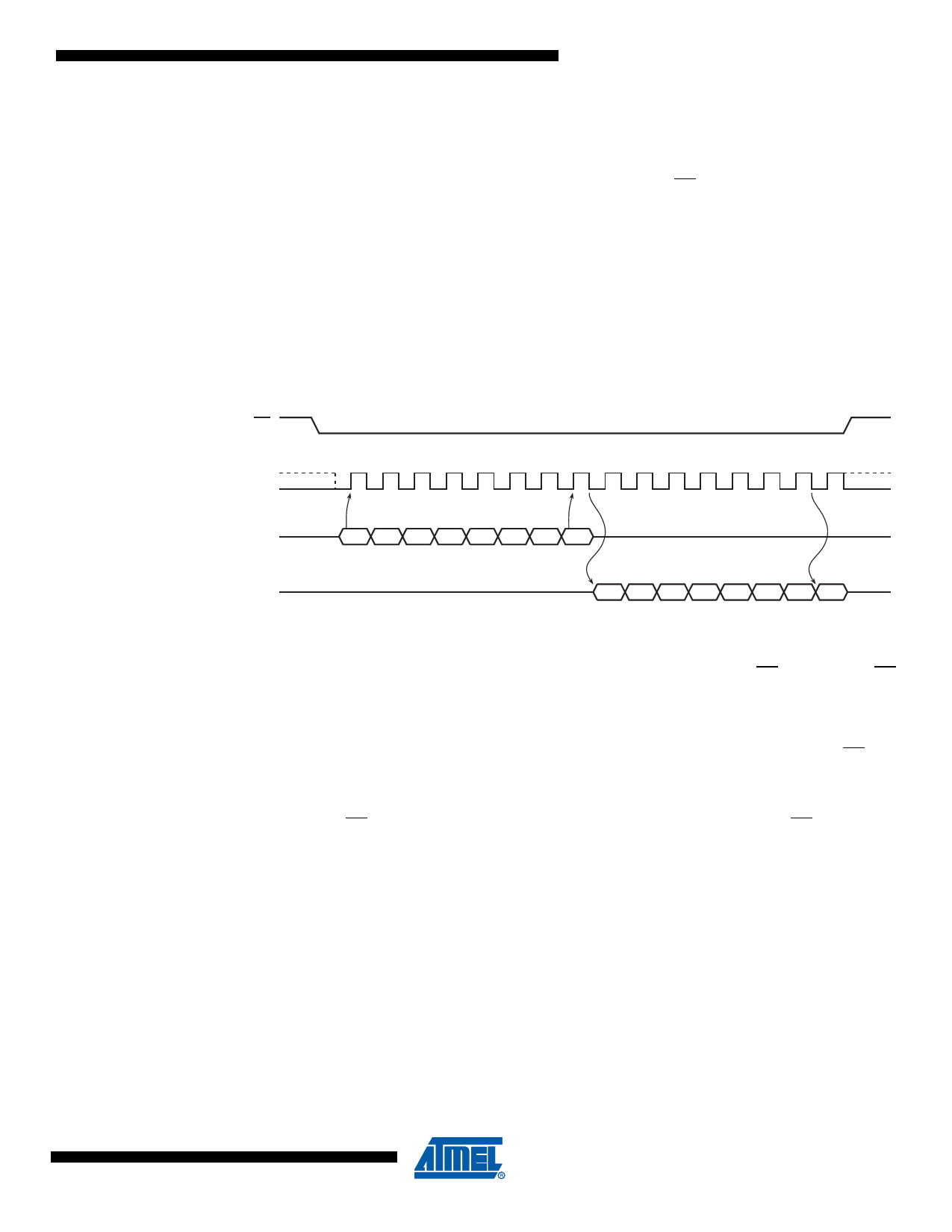
Figure 5-1. SPI Mode 0 and 3
CS
SCK
SI
MSB
LSB
SO
MSB
LSB
6. Commands and Addressing
A valid instruction or operation must always be started by first asserting the CS pin. After the CS
pin has been asserted, the host controller must then clock out a valid 8-bit opcode on the SPI
bus. Following the opcode, instruction dependent information such as address and data bytes
would then be clocked out by the host controller. All opcode, address, and data bytes are trans-
ferred with the most-significant bit (MSB) first. An operation is ended by deasserting the CS pin.
Opcodes not supported by the AT25F512B will be ignored by the device and no operation will be
started. The device will continue to ignore any data presented on the SI pin until the start of the
next operation (CS pin being deasserted and then reasserted). In addition, if the CS pin is deas-
serted before complete opcode and address information is sent to the device, then no operation
will be performed and the device will simply return to the idle state and wait for the next
operation.
Addressing of the device requires a total of three bytes of information to be sent, representing
address bits A23-A0. Since the upper address limit of the AT25F512B memory array is
00FFFFh, address bits A23-A16 are always ignored by the device.
5
3689C–DFLASH–12/08
Share Link: 