AT25D16-MH-B View Datasheet(PDF) - Atmel Corporation
Part Name
Description
Manufacturer
AT25D16-MH-B Datasheet PDF : 60 Pages
| |||
be programmed will apply. In this situation, any data that is sent to the device that goes beyond
the end of the page will wrap around back to the beginning of the same page. For example, if the
starting address denoted by A23-A0 is 0000FEh, and three bytes of data are sent to the device,
then the first two bytes of data will be programmed at addresses 0000FEh and 0000FFh while
the last byte of data will be programmed at address 000000h. The remaining bytes in the page
(addresses 000001h through 0000FDh) will not be programmed and will remain in the erased
state (FFh). In addition, if more than 256 bytes of data are sent to the device, then only the last
256 bytes sent will be latched into the internal buffer.
When the CS pin is deasserted, the device will take the data stored in the internal buffer and pro-
gram it into the appropriate memory array locations based on the starting address specified by
A23-A0 and the number of data bytes sent to the device. If less than 256 bytes of data were sent
to the device, then the remaining bytes within the page will not be programmed and will remain
in the erased state (FFh). The programming of the data bytes is internally self-timed and should
take place in a time of tPP or tBP if only programming a single byte.
The three address bytes and at least one complete byte of data must be clocked into the device
before the CS pin is deasserted, and the CS pin must be deasserted on even byte boundaries
(multiples of eight bits); otherwise, the device will abort the operation and no data will be pro-
grammed into the memory array. In addition, if the address specified by A23-A0 points to a
memory location within a sector that is in the protected state (see “Protect Sector” on page 22)
or locked down (see “Sector Lockdown” on page 29), then the Byte/Page Program command will
not be executed, and the device will return to the idle state once the CS pin has been deas-
serted. The WEL bit in the Status Register will be reset back to the logical “0” state if the
program cycle aborts due to an incomplete address being sent, an incomplete byte of data being
sent, the CS pin being deasserted on uneven byte boundaries, or because the memory location
to be programmed is protected or locked down.
While the device is programming, the Status Register can be read and will indicate that the
device is busy. For faster throughput, it is recommended that the Status Register be polled
rather than waiting the tBP or tPP time to determine if the data bytes have finished programming.
At some point before the program cycle completes, the WEL bit in the Status Register will be
reset back to the logical “0” state.
The device also incorporates an intelligent programming algorithm that can detect when a byte
location fails to program properly. If a programming error arises, it will be indicated by the EPE
bit in the Status Register.
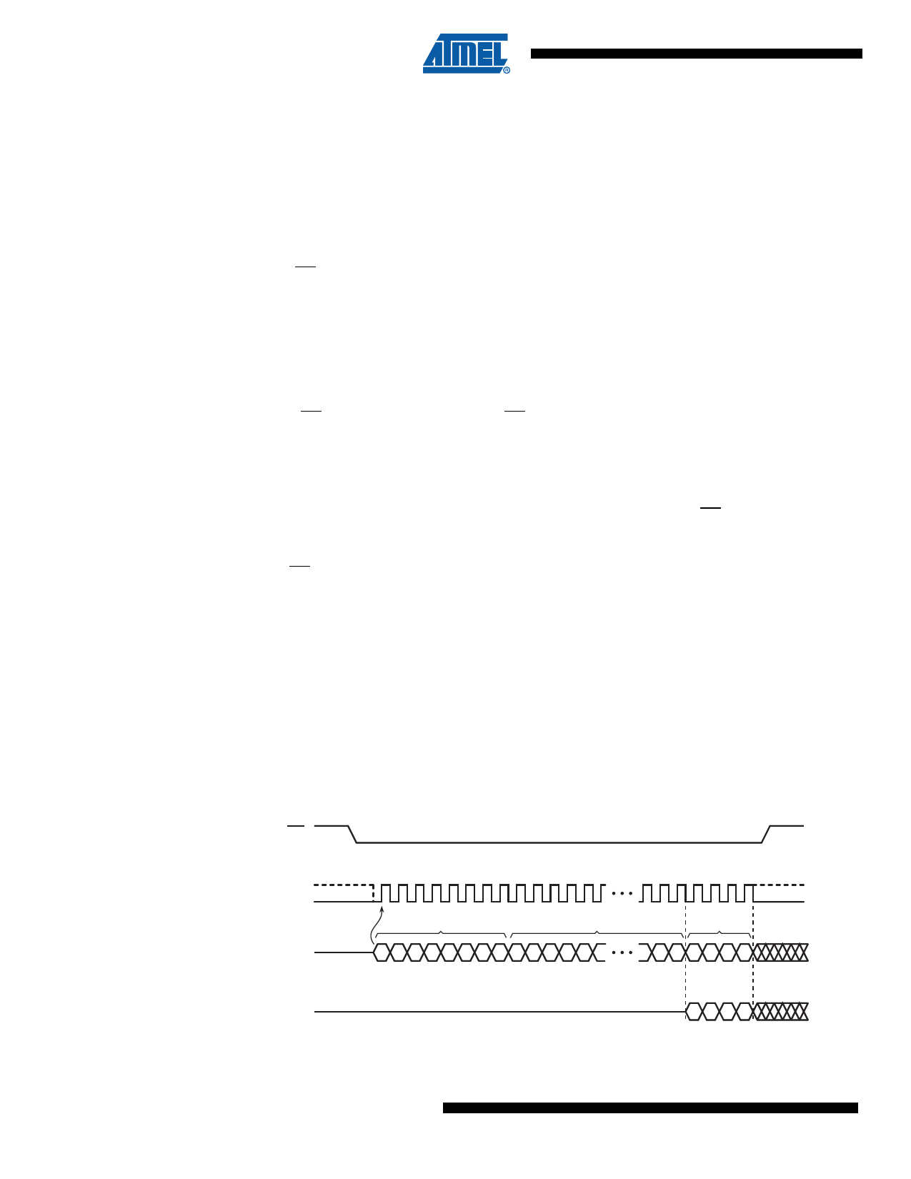
Figure 8-3. Dual-Input Byte Program
CS
SCK
SI
SOI
0 1 2 3 4 5 6 7 8 9 10 11 12
29 30 31 32 33 34 35
OPCODE
ADDRESS BITS A23-A0
INPUT
DATA BYTE
1 0 1 0 0 0 1 0AAAAAA
MSB
MSB
A A A D6 D4 D2 D0
HIGH-IMPEDANCE
D7 D5 D3 D1
MSB
14 AT25DF161 [Preliminary]
3687C–DFLASH–7/09
Share Link: 