AT45DB321E View Datasheet(PDF) - Unspecified
Part Name
Description
Manufacturer
AT45DB321E Datasheet PDF : 72 Pages
| |||
Description
The Adesto® AT45DB321E is a 2.3V minimum, serial-interface sequential access Flash memory ideally suited for a wide
variety of digital voice, image, program code, and data storage applications. The AT45DB321E also supports the RapidS
serial interface for applications requiring very high speed operation. Its 34,603,008 bits of memory are organized as
8,192 pages of 512 bytes or 528 bytes each. In addition to the main memory, the AT45DB321E also contains two SRAM
buffers of 512/528 bytes each. The buffers allow receiving of data while a page in the main memory is being
reprogrammed. Interleaving between both buffers can dramatically increase a system's ability to write a continuous data
stream. In addition, the SRAM buffers can be used as additional system scratch pad memory, and E2PROM emulation
(bit or byte alterability) can be easily handled with a self-contained three step read-modify-write operation.
Unlike conventional Flash memories that are accessed randomly with multiple address lines and a parallel interface, the
Adesto DataFlash® uses a serial interface to sequentially access its data. The simple sequential access dramatically
reduces active pin count, facilitates simplified hardware layout, increases system reliability, minimizes switching noise,
and reduces package size. The device is optimized for use in many commercial and industrial applications where
high-density, low-pin count, low-voltage, and low-power are essential.
To allow for simple in-system re-programmability, the AT45DB321E does not require high input voltages for
programming. The device operates from a single 2.3V to 3.6V power supply for the erase and program and read
operations. The AT45DB321E is enabled through the Chip Select pin (CS) and accessed via a 3-wire interface consisting
of the Serial Input (SI), Serial Output (SO), and the Serial Clock (SCK).
All programming and erase cycles are self-timed.
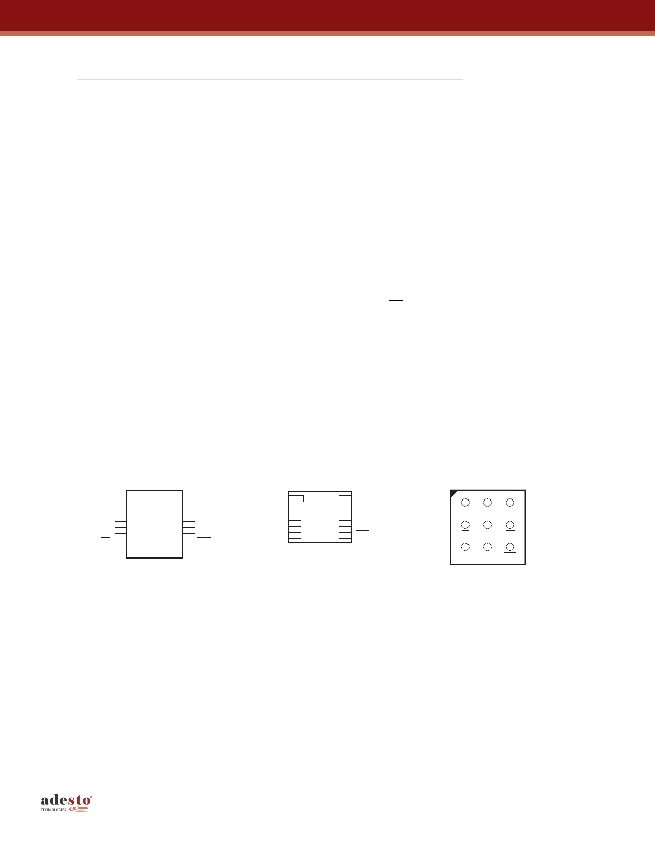
1. Pin Configurations and Pinouts
Figure 1-1. Pinouts
8-lead SOIC
Top View
SI 1
SCK 2
RESET 3
CS 4
8 SO
7 GND
6 VCC
5 WP
8-pad UDFN
Top View
(Through Package)
SI 1
SCK 2
RESET 3
CS 4
8 SO
7 GND
6 VCC
5 WP
9-ball UBGA
Top View
(Through Package)
SCK GND VCC
CS NC WP
SO
SI
RST
Note: 1. The metal pad on the bottom of the UDFN package is not internally connected to a voltage potential.
This pad can be a “no connect” or connected to GND.
AT45DB321E
2
8784E–DFLASH–10/2013
Share Link: 