ATF1516AS View Datasheet(PDF) - Atmel Corporation
Part Name
Description
Manufacturer
ATF1516AS Datasheet PDF : 11 Pages
| |||
JTAG-BST Overview
The JTAG boundary-scan testing is controlled by the Test
Access Port (TAP) controller in the ATF1516AS. The
boundary-scan technique involves the inclusion of a shift-
register stage (contained in a boundary-scan cell) adjacent
to each component so that signals at component bound-
aries can be controlled and observed using scan testing
principles. Each input pin and I/O pin has its own boundary
scan cell (BSC) in order to support boundary scan testing.
The ATF1516AS does not currently include a Test Reset
(TRST) input pin because the TAP controller is automati-
cally reset at power up. The six JTAG BST modes sup-
ported include: SAMPLE/PRELOAD, EXTEST, BYPASS,
IDCODE. BST on the ATF1516AS is implemented using
the Boundary Scan Definition Language (BSDL) described
in the JTAG specification (IEEE Standard 1149.1). Any
third party tool that supports the BSDL format can be used
to perform BST on the ATF1516AS.
The ATF1516AS also has the option of using four JTAG-
standard I/O pins for in-system programming (ISP). The
ATF1516AS is programmable through the four JTAG pins
using programming compatible with the IEEE JTAG Stan-
dard 1149.1. Programming is performed by using 5V TTL-
level programming signals from the JTAG ISP interface.
The JTAG feature is a programmable option. If JTAG (BST
or ISP) is not needed, then the four JTAG control pins are
available as I/O pins.
BSC Configuration Pins and
Macrocells (except JTAG TAP Pins)
Note: The ATF1516AS has pull-up option on TMS and TDI
pins. This feature is selected as a design option.
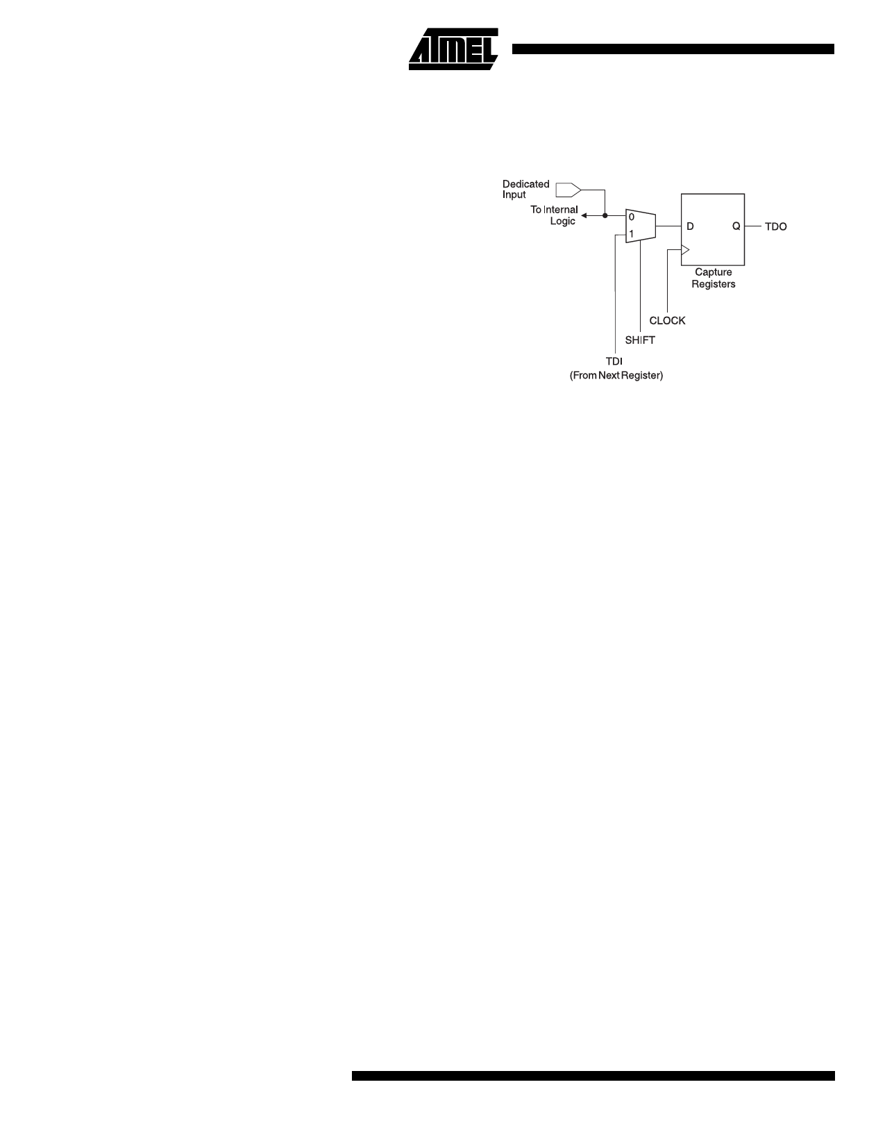
JTAG Boundary Scan Cell (BSC)
Testing
The ATF1516AS contains up to 160 I/O pins and 4 input
pins, depending on the device type and package type
selected. Each input pin and I/O pin has its own boundary
scan cell (BSC) in order to support boundary scan testing
as described in detail by IEEE Standard 1149.1. Typical
BSC consists of three capture registers or scan registers
and up to two update registers. There are two types of
BSCs, one for input or I/O pin, and one for the macrocells.
The BSCs in the device are chained together through the
capture registers. Input to the capture register chain is fed
in from the TDI pin while the output is directed to the TDO
pin. Capture registers are used to capture active device
data signals, to shift data in and out of the device and to
load data into the update registers. Control signals are gen-
erated internally by the JTAG TAP controller. The BSC
configuration for the input and I/O pins and macrocells are
shown below.
8
ATF1516AS/L
Share Link: 