TC7116CLW View Datasheet(PDF) - Microchip Technology
Part Name
Description
Manufacturer
TC7116CLW Datasheet PDF : 26 Pages
| |||
TC7116/A/TC7117/A
3.0 DETAILED DESCRIPTION
(All Pin Designations Refer to 40-Pin PDIP.)
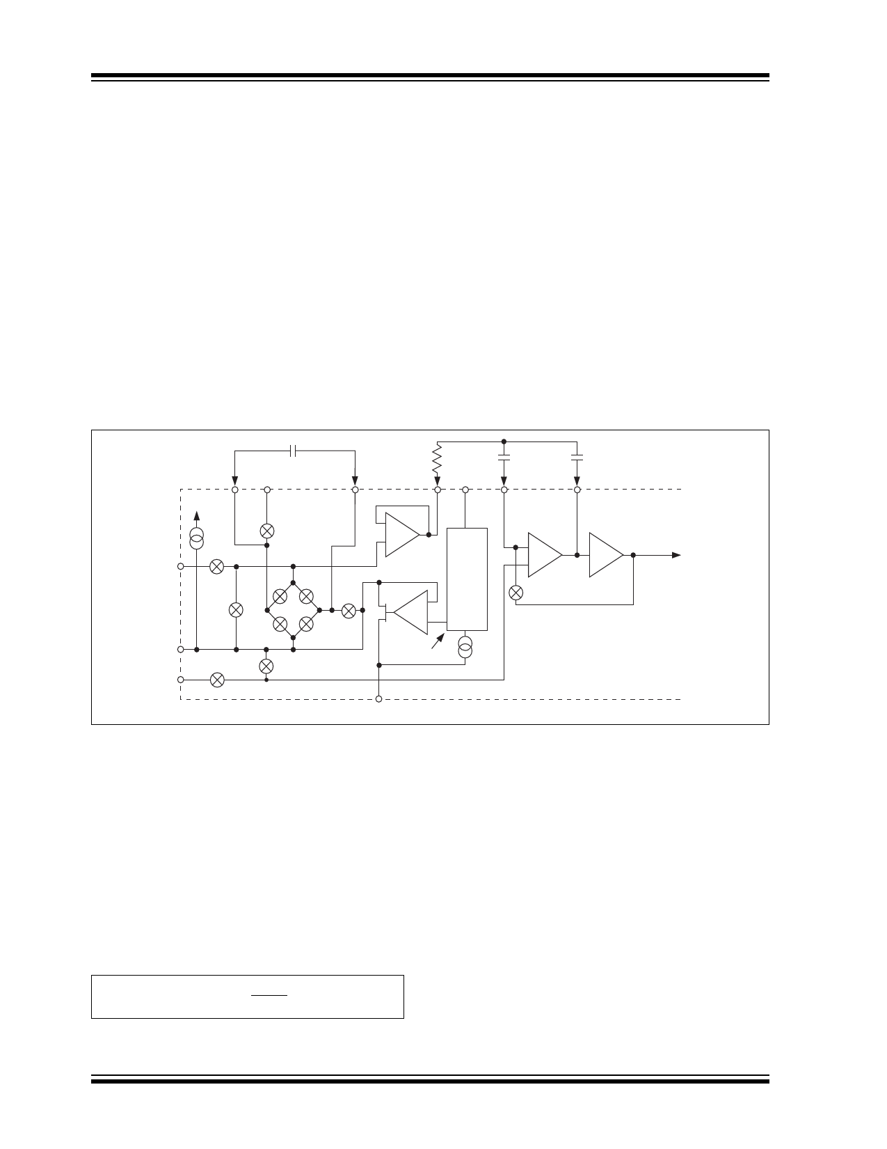
3.1 Analog Section
Figure 3-1 shows the block diagram of the analog sec-
tion for the TC7116/TC7116A and TC7117/TC7117A.
Each measurement cycle is divided into three phases:
(1) Auto-Zero (AZ), (2) Signal Integrate (INT), and
(3) Reference Integrate (REF), or De-integrate (DE).
3.1.1 AUTO-ZERO PHASE
High and low inputs are disconnected from the pins and
internally shorted to analog common. The reference
capacitor is charged to the reference voltage. A feed-
back loop is closed around the system to charge the
auto-zero capacitor (CAZ) to compensate for offset volt-
ages in the buffer amplifier, integrator, and comparator.
Since the comparator is included in the loop, AZ
accuracy is limited only by system noise. The offset
referred to the input is less than 10V.
3.1.2 SIGNAL INTEGRATE PHASE
The auto-zero loop is opened, the internal short is
removed, and the internal high and low inputs are
connected to the external pins. The converter then inte-
grates the differential voltages between VIN+ and VIN-
for a fixed time. This differential voltage can be within a
wide Common mode range: 1V of either supply. How-
ever, if the input signal has no return with respect to the
converter power supply, VIN- can be tied to analog
common to establish the correct Common mode
voltage. At the end of this phase, the polarity of the
integrated signal is determined.
CREF+
V+
CREF
VREF+
34 36
CREF-
33
10μA
VIN+ 31
INT
AZ
Analog 32
Common
VIN- 30
INT
AZ
DE DE
(–) (+)
AZ
DE (+) DE (–)
AZ & DE (±)
RINT
VBUFF
V+
28 35
–
+
Low
Temp.
Drift
Zener
–
VREF
+
V+ -3V
26
V-
CAZ
Auto-Zero
29
CINT
VINT
27
Integrator
–
+
+
Comparator
TC7116
TC7116A
TC7117
TC7117A
FIGURE 3-1:
Analog Section of TC7116/TC7116A and TC7117/TC7117A
To
Digital
Section
3.1.3 REFERENCE INTEGRATE PHASE
The final phase is reference integrate, or de-integrate.
Input low is internally connected to analog common
and input high is connected across the previously
charged reference capacitor. Circuitry within the chip
ensures that the capacitor will be connected with the
correct polarity to cause the integrator output to return
to zero. The time required for the output to return to
zero is proportional to the input signal. The digital
reading displayed is:
EQUATION 3-1:
1000 =
VIN
VREF
3.1.4 REFERENCE
The positive reference voltage (VREF+) is referred to
analog common.
DS21457D-page 8
2002-2012 Microchip Technology Inc.
Share Link: 