BD3021HFP-M View Datasheet(PDF) - ROHM Semiconductor
Part Name
Description
Manufacturer
BD3021HFP-M Datasheet PDF : 15 Pages
| |||
BD3021HFP-M
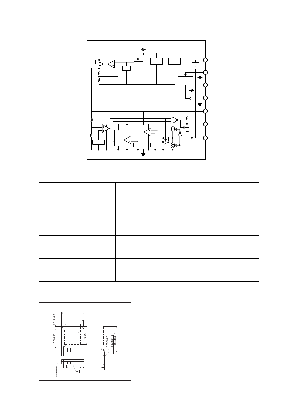
●Block diagrams
Technical Note
VREF_R
Vcc
TSD
VREF
PREREG
OCP
edge
CLK
Vcc
ON/OFF
Circuit
VREF_R
INH
Vcc
GND
VOUT
RESET
WDT
CT
VthL
VthH
Fig.13
Pin No.
1
2
3
4
5
6
7
Fin
Pin Name
CLK
INH
Vcc
GND
VOUT
RESET
CT
GND
Function
Clock Input from Microcontroller
WDT ON/OFF Function Pin
Power Supply Pin
GND
Voltage Output Pin
Reset Output Pin
External Capacitance for Reset Output Delay Time,
WDT Monitor Time Setting Connection Pin
GND
●TOP VIEW (Package dimension)
HRP7
9.395±0.125
(MAX 9.745 include BURR)
8.82±0.1
(6.5)
1.905±0.1
0.8875 1 2 3 4 5 6 7
0.73±0.1
1.27
0.08 S
4.5°
+5.5°
−4.5°
+0.1
0.27 -0.05
S
(Unit : mm)
www.rohm.com
© 2010 ROHM Co., Ltd. All rights reserved.
5/14
2010.11 - Rev.A
Share Link: 