BT856 View Datasheet(PDF) - Unspecified
Part Name
Description
Manufacturer
BT856 Datasheet PDF : 54 Pages
| |||
CIRCUIT DESCRIPTION
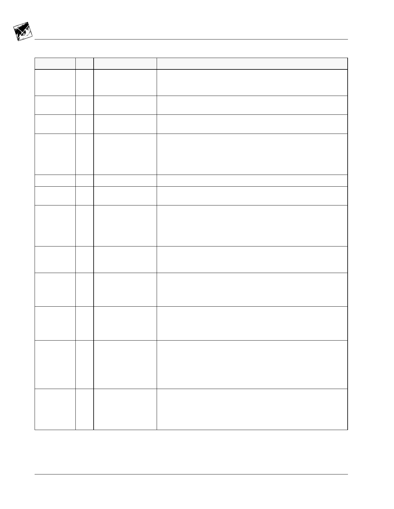
Pin Descriptions
Pin Name
SLEEP
I/O
I 44
Pin #
IIC DATA I/O 45
IIC CLOCK I 46
SLAVE
I 47
CLKX2
CLKX1
RESET*
I 48
I 49
I 52
BLANK*
I 53
VSYNC* I/O 54
HSYNC* I/O 55
SQUARE
I 58
INTERLACE I 59
Bt856/7
Description
Powerdown control input (TTL compatible). A logical one configures the
device for power-down mode. A logical zero configures the device for
normal operation. This pin may be connected directly to VAA or GND.
Serial interface data input/output (TTL compatible). Data is written to
and read from the device via this serial bus.
Serial interface clock input (TTL compatible). The maximum clock rate
is 100 kHz.
Slave/master mode select input (TTL compatible). A logical one config-
ures the device for slave video timing operation. A logical zero config-
ures the device for master video timing operation. This pin may be
connected directly to VAA or GND. This pin is ignored if bit D4 of subad-
dress register 0xDC is a logical one.
2x pixel clock input (TTL compatible).
Pixel clock input (TTL compatible). Inverted and Sampled by CLKX2 to
derive CLOCK.
Reset control input (TTL compatible). A logical zero for one CLOCK
cycle resets and disables video timing (horizontal, vertical, subcarrier
counters to the start of VSYNC of first field). A logical zero for two
CLOCK cycles also resets internal registers to 00. RESET* must be a
logical one for normal operation, commencing at the start of VSYNC.
Composite blanking control input (TTL compatible). BLANK* is regis-
tered on the rising edge of CLOCK. The R0–R7, G0–G7, and B0–B7
inputs are ignored while BLANK* is a logical zero.
Vertical sync input/output (TTL compatible). As an output (master mode
operation), VSYNC* is output following the rising edge of CLOCK. As an
input (slave mode operation), VSYNC* is registered on the rising edge
of CLOCK.
Horizontal sync input/output (TTL compatible). As an output (master
mode operation), HSYNC* is output following the rising edge of
CLOCK. As an input (slave mode operation), HSYNC* is registered on
the rising edge of CLOCK.
Square pixel/CCIR 601 resolution select input (TTL compatible). A logi-
cal one configures the device for square pixel operation. A logical zero
configures the devices for CCIR 601 resolution operation. This pin
should be connected directly to GND if using I2C. This pin is ignored if
bit D4 of subaddress register 0xDC is a logical one, or if PAL M or
N-Argentina is selected via bits D0, D1 of register 0xDA.
Interlaced/noninterlaced mode select input (TTL compatible). A logical
one configures the device for interlaced operation. A logical zero config-
ures the device for noninterlaced operation. This pin should be con-
nected directly to GND if using I2C. This pin is ignored if bit D4 of
subaddress register 0xDC is a logical one.
2
Brooktree®
Share Link: 