Q67060-S6311 View Datasheet(PDF) - Infineon Technologies
Part Name
Description
Manufacturer
Q67060-S6311 Datasheet PDF : 15 Pages
| |||
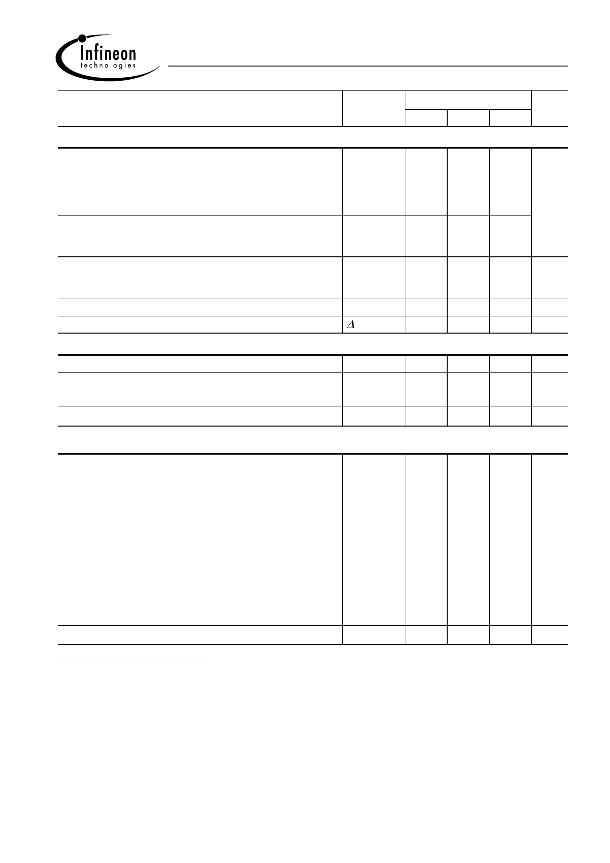
Data Sheet BTS6510
Parameter and Conditions
at Tj = -40 ... +150 °C, Vbb = 12 V unless otherwise specified
Symbol
Protection Functions
Short circuit current limit (Tab to pins 1,2,6,7)16)
VON = 12 V
Tc =-40°C:
Tc =25°C:
Output clamp 17)
(inductive load switch off)
Tc =+150°C:
IL= 40 mA:
see diagram Ind. and overvolt. output clamp page 7
Output clamp (inductive load switch off)
at VOUT = Vbb - VON(CL) (e.g. overvoltage)
IL= 40 mA
Thermal overload trip temperature
Thermal hysteresis
IL(SC)
IL(SC)
IL(SC)
-VOUT(CL)
VON(CL)
Tjt
∆Tjt
Reverse Battery
Reverse battery voltage 18)
On-state resistance (Pins 1,2,6,7 to pin 4)
Vbb = -12V, VIN = 0, IL = - 20 A, RIS = 1 kΩ
Integrated resistor in Vbb line
Tj = 25 °C:
Tj = 150 °C:
-Vbb
RON(rev)
Rbb
Values
Unit
min typ max
-- 110 --
A
45 130 180
-- 115 --
14 17 20 V
39 42 47 V
150
--
-- 10
-- °C
-- K
--
-- 32 V
-- 5.4 7.0 mΩ
8.9 12.3
-- 120
-- Ω
Diagnostic Characteristics
Current sense ratio,
static on-condition,
kILIS = IL : IIS,
VON < 1.5 V19),
VIS <VOUT - 5V,
VbIN > 4.0 V
see diagram on page 11
IL = 90 A,Tj =-40°C:
Tj =25°C:
Tj =150°C:
IL = 20 A,Tj =-40°C:
Tj =25°C:
Tj =150°C:
IL = 10 A,Tj =-40°C:
Tj =25°C:
Tj =150°C:
IL = 4 A,Tj =-40°C:
Tj =25°C:
Tj =150°C:
IIS=0 by IIN =0 (e.g. during deenergizing of inductive loads):
Sense current saturation
kILIS
IIS,lim
12 400 14 200 16 000
12 000 13 700 15 400
11 400 12 800 14 200
12 200 14 800 17 400
12 000 14 100 16 200
11 500 13 200 15 000
11 100 15 300 19 500
11 500 14 500 17 500
11 400 13 300 15 200
10 000 17 600 28 500
11 000 15 600 22 000
10 600 13 800 18 000
6.5
--
-- mA
16 ) Short circuit is a failure mode. The device is not designed to operate continuously into a short circuit. The
lifetime will be reduced under such conditions.
17) This output clamp can be "switched off" by using an additional diode at the IS-Pin (see page 7). If the diode
is used, VOUT is clamped to Vbb- VON(CL) at inductive load switch off.
18) The reverse load current through the intrinsic drain-source diode has to be limited by the connected load (as
it is done with all polarity symmetric loads). Note that under off-conditions (IIN = IIS = 0) the power transistor
is not activated. This results in raised power dissipation due to the higher voltage drop across the intrinsic
drain-source diode. The temperature protection is not active during reverse current operation! Increasing
reverse battery voltage capability is simply possible as described on page 8.
19) If VON is higher, the sense current is no longer proportional to the load current due to sense current
saturation, see IIS,lim .
Infineon Technologies AG
Page 5 of 15
2000-Mar-29
Share Link: 