S80C851-4N44 View Datasheet(PDF) - Philips Electronics
Part Name
Description
Manufacturer
S80C851-4N44 Datasheet PDF : 22 Pages
| |||
Philips Semiconductors
CMOS single-chip 8-bit microcontroller
with on-chip EEPROM
Product specification
80C851/83C851
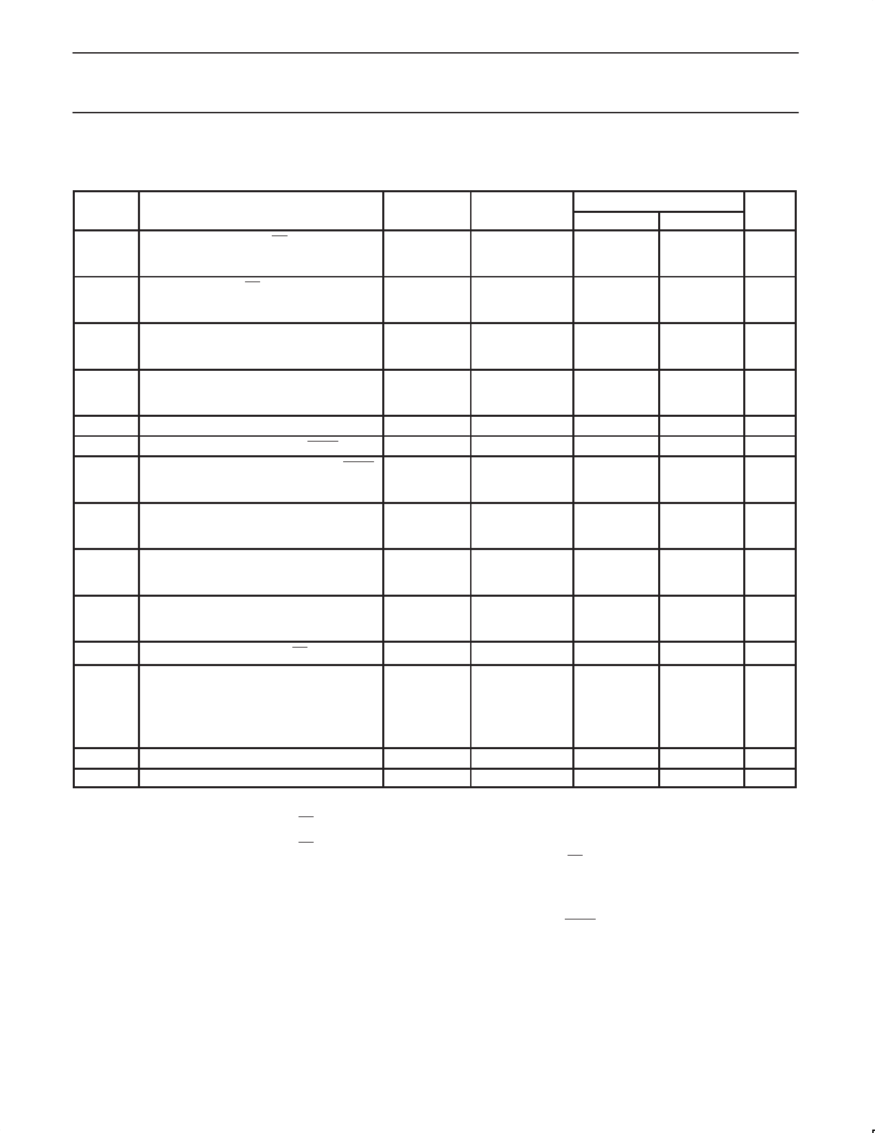
DC ELECTRICAL CHARACTERISTICS
Tamb = 0°C to +70°C (VDD = 5V ±10%), –40°C to +85°C (VDD = 5V ±10%), or –40°C to +125°C (VDD = 5V ±10%), VSS = 0V
PART
TEST
LIMITS
SYMBOL
PARAMETER
TYPE
CONDITIONS
MIN
MAX
UNIT
VIL
VIL1
VIH
VIH1
VOL
VOL1
VOH
VOH1
IIL
Input low voltage, except EA
0 to +70°C
–40 to +85°C
–40 to +125°C
–0.5
–0.5
–0.5
0.2VDD–0.1
V
0.2VDD–0.15
V
0.2VDD–0.25
V
Input low voltage to EA
0 to +70°C
–40 to +85°C
–40 to +125°C
–0.5
–0.5
–0.5
0.2VDD–0.3
V
0.2VDD–0.35
V
0.2VDD–0.45
V
Input high voltage, except XTAL1, RST
0 to +70°C
–40 to +85°C
–40 to +125°C
0.2VDD+0.9
VDD+0.5
V
0.2VDD+1.0
VDD+0.5
V
0.2VDD+1.0
VDD+0.5
V
Input high voltage, XTAL1, RST
0 to +70°C
–40 to +85°C
–40 to +125°C
0.7VDD
0.7VDD+0.1
0.7VD+0.1
VDD+0.5
VDD+0.5
VDD+0.5
Output low voltage, ports 1, 2, 3 6
Output low voltage, port 0, ALE, PSEN 6
IOL = 1.6mA4
IOL = 3.2mA4
0.45
V
0.45
V
Output high voltage, ports 1, 2, 3, ALE, PSEN
IOH = –60µA,
2.4
V
IOH = –25µA,
0.75VDD
V
IOH = –10µA
0.9VDD
V
Output high voltage, port 0 in external bus
IOH = –800µA,
2.4
V
mode5
IOH = –300µA,
0.75VDD
V
IOH = –80µA
0.9VDD
V
Logical 0 input current, ports 1, 2, 3
0 to +70°C
–40 to +85°C
–40 to +125°C
VIN = 0.45V
–50
µA
–75
µA
–75
µA
ITL
Logical 1-to-0 transition current, ports 1, 2, 3
0 to +70°C
VIN = 2.0V
–40 to +85°C
–40 to +125°C
–650
µA
–750
µA
–750
µA
IL1
Input leakage current, port 0, EA
0.45V<Vi<VDD
±10
µA
IDD
Power supply current:
Active mode @ 16MHz 1
Active mode @ 24MHz 1
Idle mode @ 16MHz 2
Idle mode @ 24MHz 2
Power down mode 3
See note 7
19
mA
29
mA
3.7
mA
5.6
mA
50
µA
RRST
Internal reset pull-down resistor
50
150
kΩ
CIO
Pin capacitance
f = 1MHz
10
pF
NOTES:
1. The operating supply current is measured with all output pins disconnected; XTAL1 driven with tr = tf = 5ns; VIL = VSS +0.5V;
VIH = VDD – 0.5V; XTAL2 not connected; EA = RST = Port 0 = VDD.
2. The idle mode supply current is measured with all output pins disconnected; XTAL1 driven with tr = tf = 5ns; VIL = VSS +0.5V;
VIH = VDD – 0.5V; XTAL2 not connected; EA = Port 0 = VDD; RST = VSS.
3. The power-down current is measured with all output pins disconnected; XTAL2 not connected; EA = Port 0 = VDD; RST = XTAL1 = VSS.
4. Capacitive loading on Port 0 and Port 2 may cause spurious noise pulses to be superimposed on the LOW level output voltage of ALE, Port
1 and Port 3. The noise is due to external bus capacitance discharging into the Port 0 and Port 2 pins when these pins make a 1-to-0
transition during bus operations. In the worst cases (capacitive loading > 100pF), the noise pulse on the ALE line may exceed 0.8V. In such
cases it may be desirable to qualify ALE with a Schmitt Trigger, or use an address latch with a Schmitt Trigger STROBE input.
5. Capacitive loading on Port 0 and Port 2 may cause the HIGH level output voltage on ALE and PSEN to momentarily fall below the 0.9VDD
specification when the address bits are stabilizing.
6. Under steady state (non-transient) conditions, IOL must be externally limited as follows:
Maximum IOL per Port pin:
10mA
Maximum IOL per 8-bit port –
Port 0: 26mA
Ports 1, 2, and 3: 15mA
Maximum total IOL for all output pins: 71mA.
If IOL exceeds the test condition, VOL may exceed the related specification. Pins are not guaranteed to sink current greater than the listed
test conditions.
7. See Figures 11 through 14 for IDD test conditions.
1998 Jul 03
11
Share Link: 