C8051F231 View Datasheet(PDF) - Silicon Laboratories
Part Name
Description
Manufacturer
C8051F231 Datasheet PDF : 2 Pages
| |||
C8051F231
25 MIPS, 8 kB Flash, 32-Pin Mixed-Signal MCU
Analog Peripherals
Two comparators
- Programmable hysteresis
- Configurable to generate interrupts or reset
VDD Monitor and Brown-out Detector
On-Chip JTAG Debug
- On-chip emulation circuitry facilitates full-speed, non-intrusive, in-circuit
emulation
- Supports breakpoints, single stepping, watchpoints, inspect/modify
memory, and registers
- Superior performance to emulation systems using ICE-chips, target
pods, and sockets
- Fully compliant with IEEE 1149.1 specification
Supply Voltage: 2.7 to 3.6 V
- Typical operating current: 9 mA at 25 MHz
- Typical stop mode current: <0.1 µA
Temperature Range: –40 to +85 °C
High-Speed 8051 µC Core
- Pipelined instruction architecture; executes 70% of instructions in 1 or 2
system clocks
- Up to 25 MIPS throughput with 25 MHz system clock
- Expanded interrupt handler; up to 21 interrupt sources
Memory
- 256 bytes data RAM
- 8 kB Flash; in-system programmable in 512 byte sectors (512 bytes are
reserved)
Digital Peripherals
- 22 port I/O; all are 5 V tolerant
- Hardware SPI™ and UART serial ports available concurrently
- 3 general-purpose 16-bit counter/timers
- Dedicated watchdog timer; bidirectional reset
Clock Sources
- Internal programmable oscillator: 2–16 MHz
- External oscillator: Crystal, RC, C, or Clock
- Can switch between clock sources on-the-fly
Package
- 32-pin LQFP (standard lead and lead-free packages)
Part Ordering Numbers
- Lead-free package: C8051F231-GQ
- Standard package: C8051F231
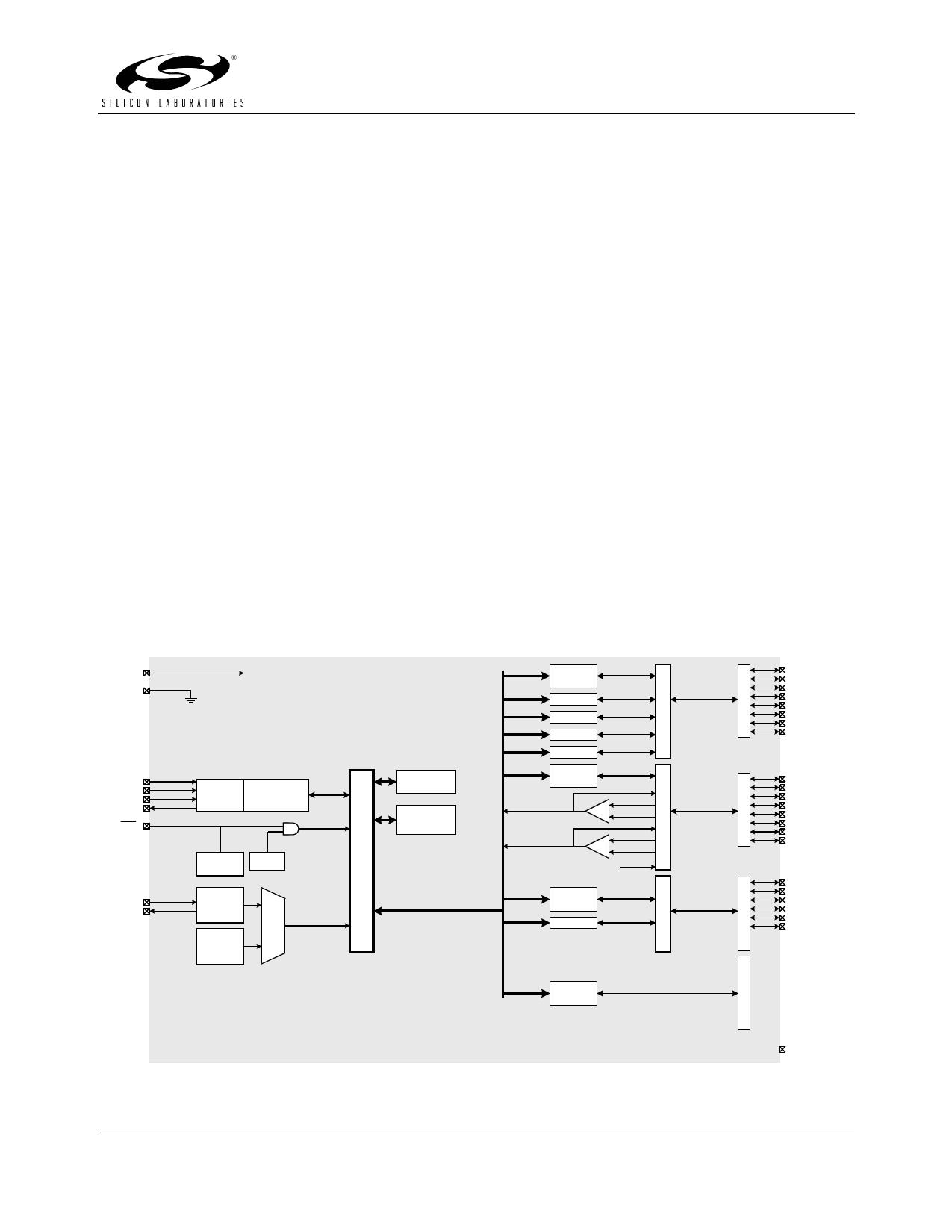
VDD
GND
Analog/Digital
Power
TCK
TMS
TDI
TDO
RST
XTAL1
XTAL2
JTAG
Logic
VDD
Monitor
External
Oscillator
Circuit
Internal
Oscillator
Debug HW
8
0
5 Reset
1
WDT
C
o
r System Clock
e
8 kB FLASH
256 byte
RAM
SFR Bus
Port 0
Latch
P
UART
0
Timer 0
M
U
Timer 1
X
Timer 2
Port 1
Latch
CP0
CP0
CP1
CP1
P
CP0+
1
CP0-
M
CP1+
U
X
CP1-
SYSCLK
P
Port 2
2
Latch
SPI
M
U
X
Port 3
Latch
P
P0.0/TX
P0.1/RX
0
P0.2//INT0
P0.3//INT1
D
P0.4/T0
r
P0.5/T1
v
P0.6/T2
P0.7/T2EX
P
P1.0/CP0+
P1.1/CP0-
1
P1.2/CP0
P1.3/CP1+
D
P1.4/CP1-
r
P1.5/CP1
v
P1.6/SYSCLK
P1.7
P
P2.0/SCK
P2.1/MISO
2
P2.2/MOSI
P2.3/NSS
D
P2.4
r
P2.5
v
P
3
D
r
v
NC
General Purpose
Copyright © 2005 by Silicon Laboratories
5.5.2005
Share Link: 