CA3060 View Datasheet(PDF) - Intersil
Part Name
Description
Manufacturer
CA3060 Datasheet PDF : 12 Pages
| |||
CA3060
Electrical Specifications TA = 25oC, VSUPPLY = ±15V (Continued)
AMPLIFIER BIAS CURRENT
PARAMETER
SYMBOL
IABC = 1µA
MIN TYP MAX
IABC = 10µA
MIN TYP MAX
IABC = 100µA
MIN TYP MAX UNITS
Input Impedance Components
Resistance (See Figure 14)
RI
-
1600
-
-
170
-
10
20
-
kΩ
Capacitance at 1MHz
CI
-
2.7
-
-
2.7
-
-
2.7
-
pF
Output Impedance Components
Resistance (See Figure 15)
RO
-
200
-
-
20
-
-
2
-
MΩ
Capacitance at 1MHz
CO
-
4.5
-
-
4.5
-
-
4.5
-
pF
ZENER BIAS REGULATOR CHARACTERISTICS I2 = 0.1mA
Voltage (See Figure 16)
VZ
Temperature
6.2
6.7
7.9
Coefficient = 3mV/oC
V
Impedance
ZZ
NOTES:
-
200 300
Ω
3. Conditions for Input Offset Voltage Sensitivity:
a. Bias current derived from the regulator with an appropriate resistor connected from Terminal 1 to the bias terminal on the amplifier
under test V+ is reduced to +13V for V+ sensitivity and V- is reduced to -13V for V- sensitivity.
b. V+ Sensitivity in µV ⁄ V = V-----O-----f--f--s---e----t---–-----V----O-----f--f--s----e----t---f--o---r--1--+--V--1---3---V------a---n----d--------1---5---V------S----u---p----p---l-i--e---s-- ,
V- Sensitivity in µV ⁄ V = V-----O-----f--f--s---e----t---–-----V----O-----f--f--s----e----t---f--o---r--1-----V1---3----V-----a----n---d-----+----1---5---V------S----u---p----p---l-i--e---s--.
4. Temperature Coefficient; -2.2mV/oC (at VABC = 0.54, IABC = 1µA); -2.1mV/oC (at VABC = 0.060V, IABC = 10µA); -1.9mV/oC (at VABC = 0.66V,
IABC = 100µA)
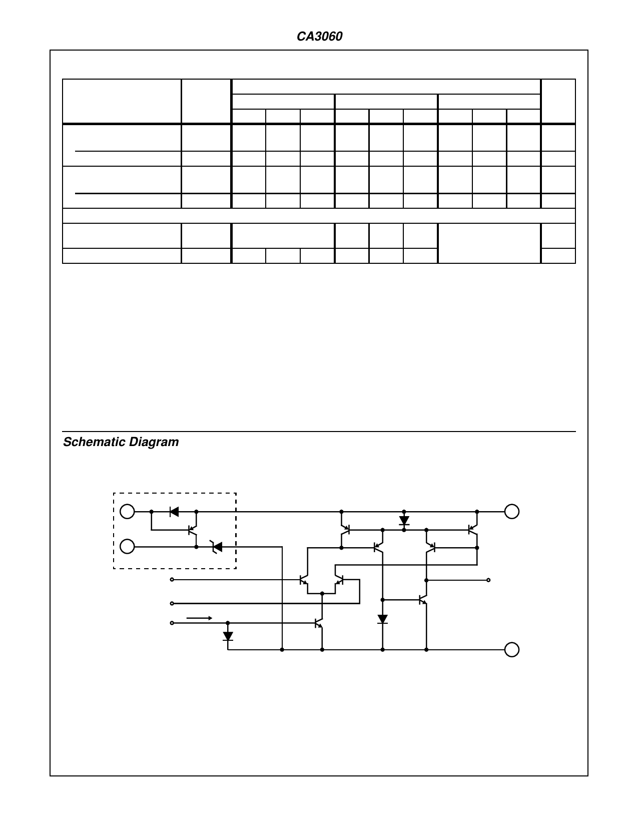
Schematic Diagram
BIAS REGULATOR AND ONE OPERATIONAL TRANSCONDUCTANCE AMPLIFIER
ZENER BIAS REGULATOR
D4
2
Q10
1
D5
INVERTING INPUT -
(NOTE 5)
NON-INVERTING INPUT +
(NOTE 6)
IABC
AMPLIFIER BIAS INPUT
(NOTE 7)
D1
Q4
Q1 Q2
Q3
D2
Q6
Q7
Q8
D3
NOTES:
5. Inverting Input of Amplifiers 1, 2 and 3 is on Terminals 13, 12 and 4, respectively.
6. Non-inverting Input of Amplifiers 1, 2 and 3 is Terminals 14, 11 and 5, respectively.
7. Amplifier Bias Current of Amplifiers 1, 2 and 3 is on Terminals 15, 10 and 6, respectively.
8. Output of Amplifiers 1, 2 and 3 is on Terminals 16, 9 and 7, respectively.
3 V+
Q5
OUTPUT (NOTE 8)
8 V-
3-3
Share Link: 