COM20051 View Datasheet(PDF) - SMSC -> Microchip
Part Name
Description
Manufacturer
COM20051
SMSC -> Microchip

COM20051 Datasheet PDF : 92 Pages
| |||
Clock Speed
Emulate Mode
The COM20051+ processor operates at 16MHz
and the network controller at a maximum
40MHz clock rate. A single crystal oscillator is
used to supply the two clocks: a 16MHz
processor clock and a 20MHz network clock for
the nominal 2.5 Mbps data rate. Pins 29 and 30
are designated as crystal inputs. When clocking
with an external oscillator, pin 30 (XTAL1)
functions as the clock input.
The COM20051+ contains a unique feature
called the Emulate mode that most 8051-based
peripheral devices do not accommodate. The
Emulate mode permits developers to access
and program the internal ARCNET core using a
standard low-cost 8032 emulator. This feature
eliminates the need for expensive dedicated
development equipment needed for other types
of 8051-based peripheral devices. The Emulate
mode is invoked by connecting the nEA/EMUL
pin to VCC. This causes the internal 80C32
processor to enter a HI-Z state and changes the
state of the COM20051+ pins according to the
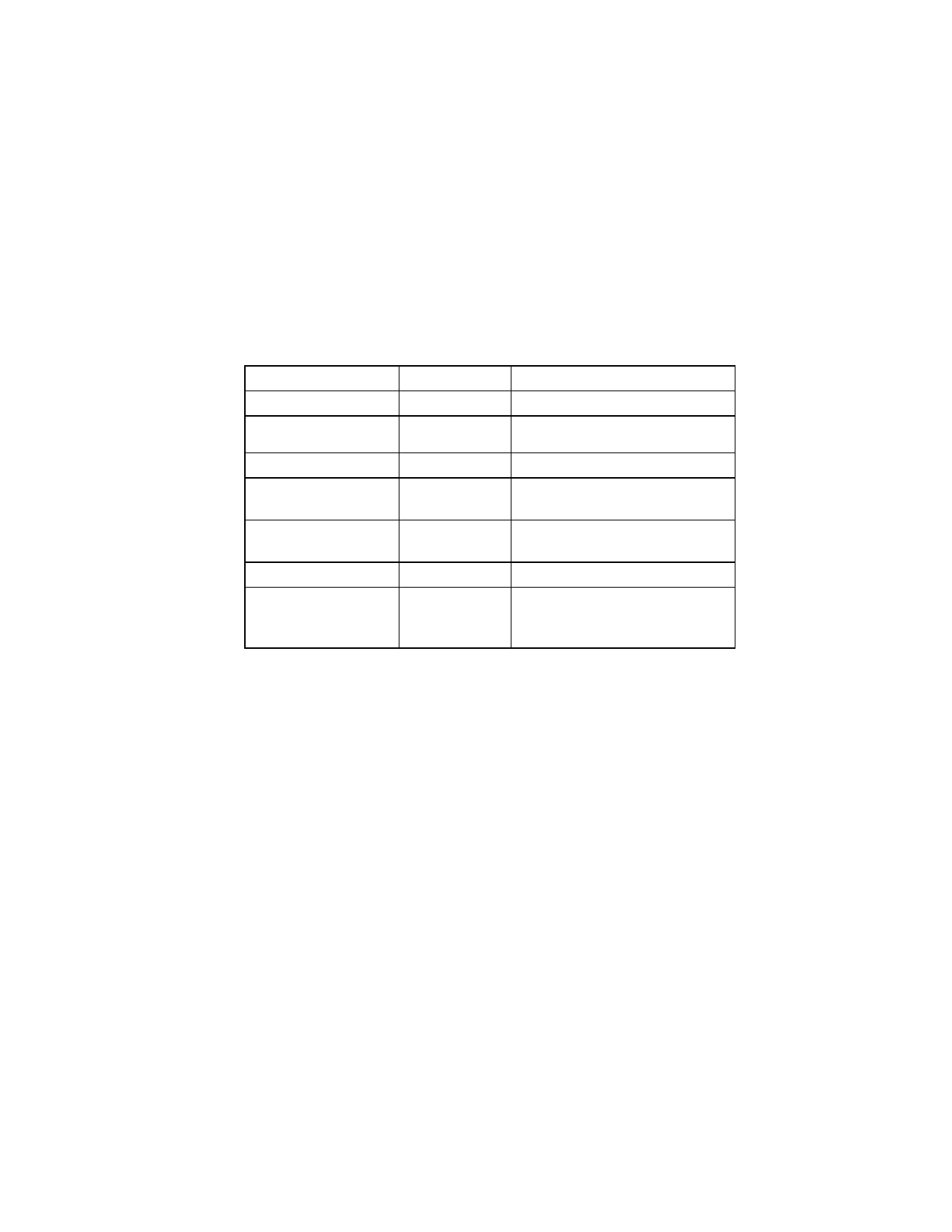
following table:
SIGNAL NAME
PORT 0
PORT 1
PORT 2
INT0,1
(P3.2, P3.3)
RD/WR
(P3.6, P3.7)
ALE
TX,T0, T1
(P3.1,3.4,3.5)
nPSEN
Table 1 - Emulate Mode
EMUL = 0
EMUL = 1
Bidirectional Bidirectional
Bidirectional
Output
HI-Z (except for pins designated
as interrupt destinations)
Input
Input
Output
Output
Input
Output
Output
Input
HI-Z
Address Decoding
The COM20051+, as described previously,
maps the peripheral function registers into the
80C32's External Data Memory space. This
provides system flexibility because the location
of the peripheral registers can be located
anywhere within the 64K External Data Memory
space. The precise location can be resolved
with a 256-byte page.
The location of that page in the External Data
Memory space is pointed to by the Address
Decode Register, as shown in Figure 2. The
Address Decode Register is located at FFFFh of
the External Data Memory space. It holds the
upper 8 bits of the 16-bit address at which the
256 page boundary will start. This register must
be programmed prior to any access to the
ARCNET core. The default value is 0000h.
9
Share Link: