CXA1898Q View Datasheet(PDF) - Sony Semiconductor
Part Name
Description
Manufacturer
CXA1898Q Datasheet PDF : 26 Pages
| |||
3. AMS
(1) AMS output logic
Detection status
AMS OUT (Pin 2)
Signal detection No signal detection
L
H
AMS OUT (Pin 2) is an open collector output pin. When a 2.2kΩ resistor is connected to VDD:
Low : approximately 0.5V (IOL = 2mA (max.))
High : VDD
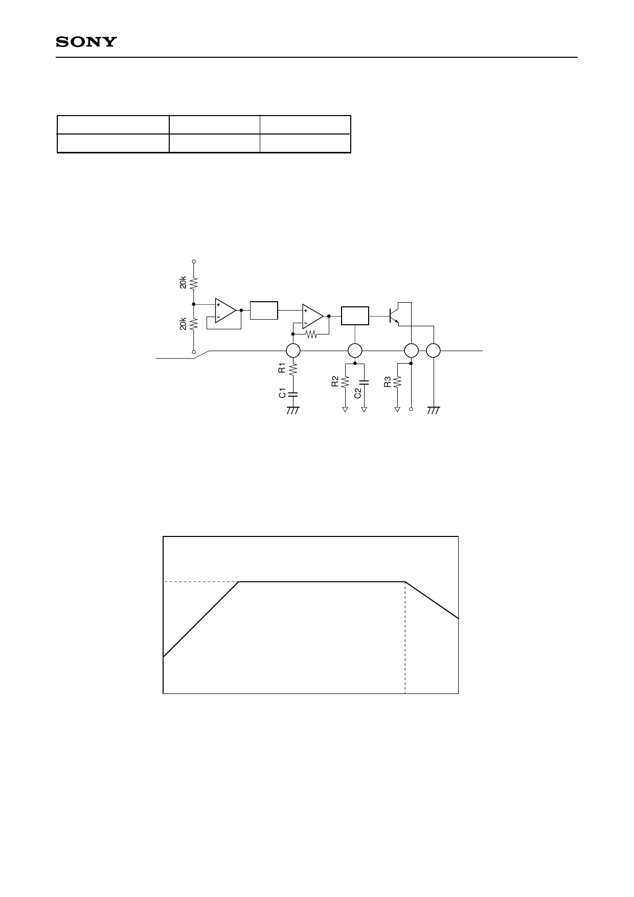
Fig. 1 shows the AMS block diagram.
PB OUT1
Inside IC
PB OUT2
SA
HPF
LPF
25kHz
AMS GAIN 100k
48
DET
1 AMS OUT 2
AMS FIL
AMS GND
3
CXA1898Q
GND
VDD VDD
VDD
GND
Fig. 1 AMS Block Diagram
Fig. 2 shows the frequency response of the signal output from HPF.
fC
G
GAIN
(dB)
10
1kHz
25kHz
100kHz
f (Hz)
Fig. 2 Frequency Response
– 20 –
Share Link: 