CXA2581 View Datasheet(PDF) - Sony Semiconductor
Part Name
Description
Manufacturer
CXA2581 Datasheet PDF : 22 Pages
| |||
CXA2581N
Description of Functions
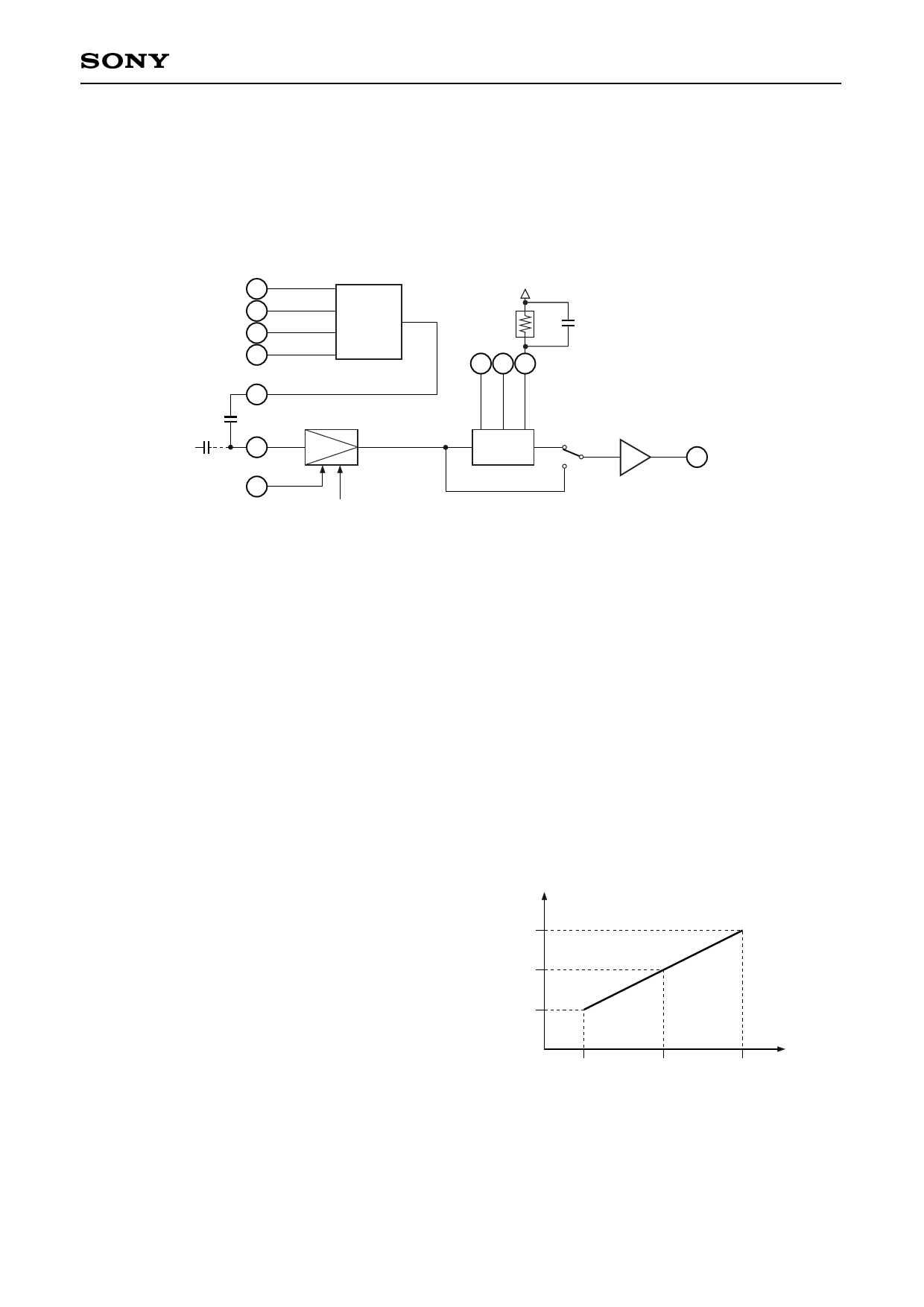
• RFAC
The RF signal input by connecting capacitance to the EQ_IN pin is equalized, arithmetically amplified and then
output from the RFAC pin.
A6
B7
C8
D9
AC_SUM 4
AC
SUM
VCC
5.1k 0.1µ
BST VFC
24 25 26 RFC
RF
3
EQ_IN
RFG 23
RW/ROM
EQ
BST = VCC
Amp
15 RFAC
Low frequency gain
AC_SUM:
13dB (both ROM/RW)
VCA to RFAC ROM: 0dB
RW: 12dB
The EQ can be bypassed by connecting the BST control pin (Pin 24) to VCC.
In this case only the EQ block enters sleep mode and low power consumption mode (slim mode) is activated.
The low frequency gain is the same value as for EQ ON mode.
If RF (summing signal) is present at the pickup output pin, input the addition output signal to EQ_IN (Pin 3)
coupled by capacitance.
When using a pickup without a summing output function, perform addition with the AC SUM block and then
input the signal to EQ_IN (Pin 3) coupled by capacitance.
RW/ROM switching is done by the VCA block, so either input method can be used without problem.
The RW gain is 12dB higher than the ROM gain.
The VCA low frequency gain can be adjusted by the RFG
(Pin 23) voltage.
The control voltage vs. low frequency gain characteristics
are shown in the graph to the right.
Gain [dB]
8
0
VCA variable range
–8
Vcnt
[V]
VC – 1
VC
VC + 1
The RFAC pin (Pin 15) is an NPN transistor emitter follower output.
The maximum drive current is approximately 2mA.
If the load capacitance distorts the output waveform, connect resistance between Pin 15 and GND to increase
the drive current.
–9–
Share Link: 