CXA3562AR View Datasheet(PDF) - Sony Semiconductor
Part Name
Description
Manufacturer
CXA3562AR Datasheet PDF : 24 Pages
| |||
CXA3562AR
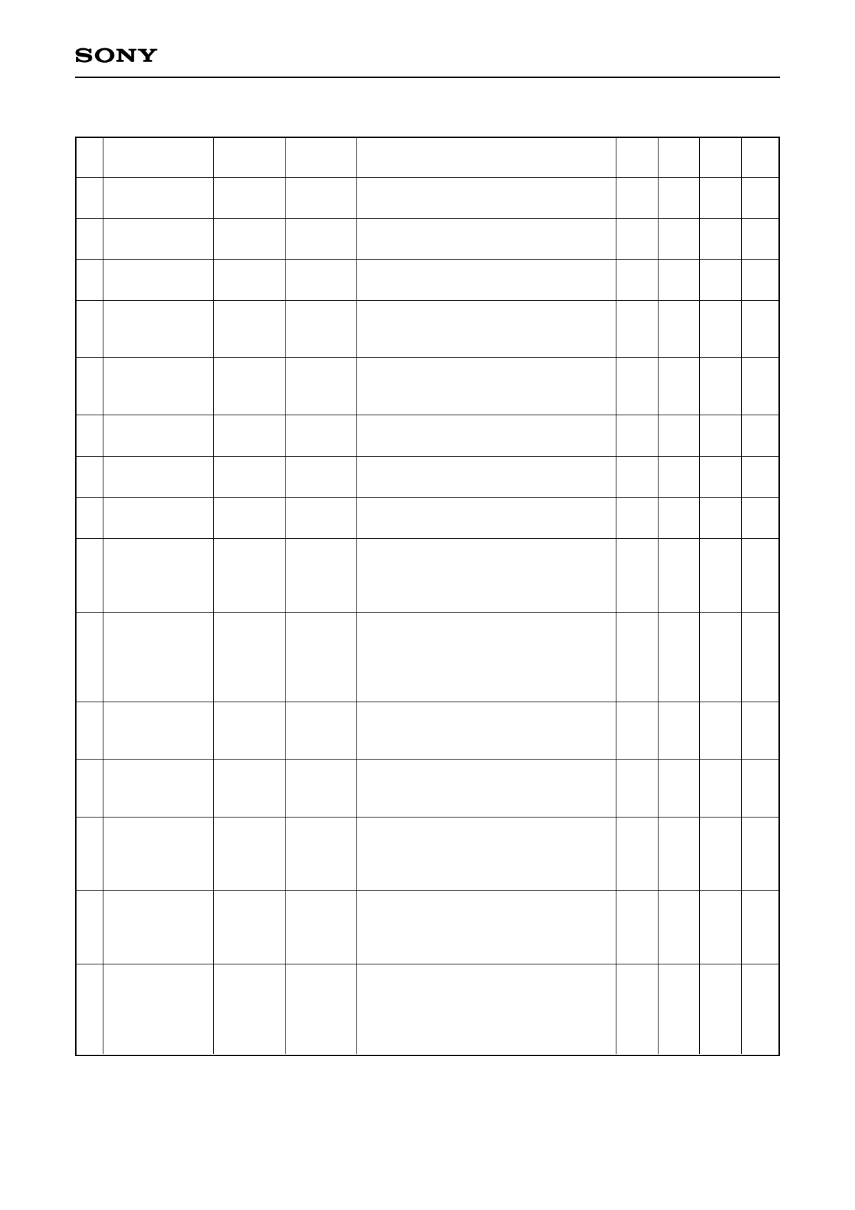
Electrical Characteristics
No.
Item
Symbol
Measurement
points
Measurement conditions
Min. Typ. Max. Unit
1
Digital input
resolution
n
— 10 — bit
2
Digital input
setup time
TS
SHST, D_A[9:0] and D_B[9:0] minimum
setup time relative to MCLK input. (PELL)
2
— — ns
3
Digital input
hold time
TH
SHST, D_A[9:0] and D_B[9:0] minimum
hold time relative to MCLK input. (PECL)
3
— — ns
MCLK input
4 frequency
range 1
fMCLK1
SL_DAT: 5V; maximum frequency at
which the internal timing generator
and D/A converter operate normally.
30 — 80 MHz
MCLK input
5 frequency
range 2
fMCLK2
SL_DAT: 0V; maximum frequency at
which the internal timing generator
and D/A converter operate normally.
60 — 100 MHz
6
VREF_O output
voltage range
VVREF_O
Measure the VREF_O (Pin 69)
voltage.
3.10 3.20 3.32 V
7
SH_OUT
amplitude 1
VSHOUT1p-p VOUT1
Measure the SH_OUT1 voltage
difference at D_A[9:0]: 000h and 3FFh.
4.44 4.50 4.83
V
8
SH_OUT
amplitude 2
VSHOUT2p-p VOUT2
Measure the SH_OUT2 voltage
difference at D_B[9:0]: 000h and 3FFh.
4.44 4.50 4.83
V
SH_OUT
9 minimum
amplitude
VOUTMINp-p VOUT1
Lower the VREF_I voltage and adjust
the amplitude; minimum amplitude at
which SH_OUT1 can be output at
4
——
V
D_B[9:0]: 000h and 3FFh.
10
SH_OUT
slew rate
SROUT
VOUT1 to
VOUT12
Load capacitance = 360pF; measure
slew rate at 10 to 90% of output
waveform rise and fall when D_A[9:0] 160 300
is varied from 000h to 3FFh and from
3FFh to 000h.
— V/µs
SH_OUT
11 minimum
VMIN
output voltage
VOUT1 to
VOUT12
Minimum voltage at which sample-
and-hold outputs VOUT1 to VOUT12 can
be output.
1.5
—
—
V
SH_OUT
12 maximum
output voltage
VMAX
VOUT1 to
VOUT12
Maximum voltage at which sample-
and-hold outputs VOUT1 to VOUT12 can
be output.
—
— 13.6 V
Output deviation
13 between
channels 1
DOUT1
Value obtained by subtracting minimum
VOUT1 to
VOUT12
VOUT1 to VOUT12 value from maximum
VOUT1 to VOUT12 value at D_A[9:0]: 200h
—
3
10 mVp-p
and D_B[9:0]: 200h.
Output deviation
14 between
channels 2
DOUT2
Value obtained by subtracting minimum
VOUT1 to
VOUT12
VOUT1 to VOUT12 value from maximum
VOUT1 to VOUT12 value at D_A[9:0]: 000h
—
10
40 mVp-p
or 3FFh and D_B[9:0]: 000h or 3FFh.
15
Output deviation
between ICs 1
DIC1
Value obtained by subtracting minimum
VOUT1 to
VOUT12
VOUT1 to VOUT12 value from maximum
VOUT1 to VOUT12 value at D_A[9:0]: 200h
and D_B[9:0]: 200h. (when using two
—
10
— mVp-p
CXA3562R)
–9–
Share Link: 