CXD3609R View Datasheet(PDF) - Sony Semiconductor
Part Name
Description
Manufacturer
CXD3609R Datasheet PDF : 72 Pages
| |||
CXD3609R
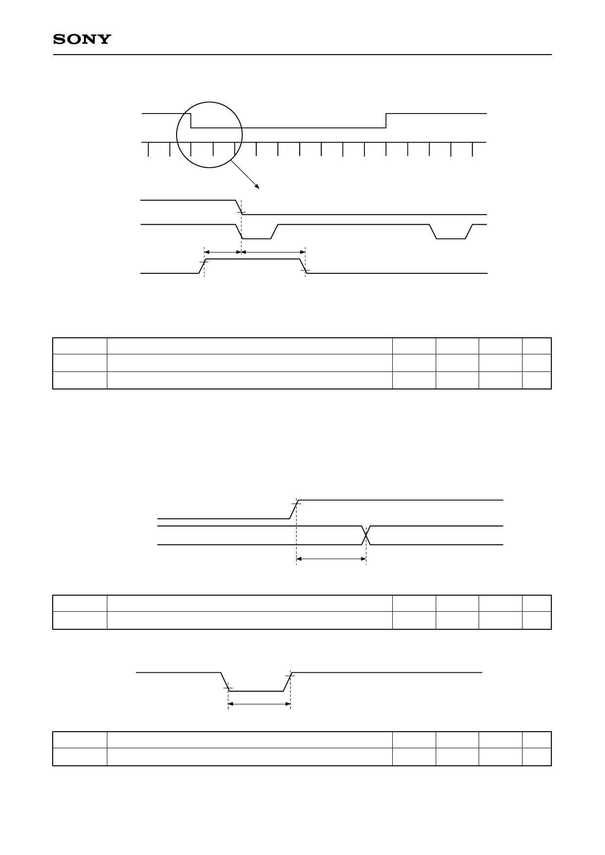
Serial interface clock internal loading characteristics (2)
Example: During progressive scan (high-speed sweep present)
VR
HR
Enlarged view
VR
0.2VDDc
HR
SEN
ts1
0.8VDDc
th1
0.2VDDc
∗ Be sure to maintain a constantly high SEN logic level near the falling edge of VR.
(Within the recommended operating conditions)
Symbol
ts1
th1
Definition
SEN setup time, activated by the falling edge of VR
SEN hold time, activated by the falling edge of VR
Min. Typ. Max. Unit
0
ns
200
ns
Serial interface clock output variation characteristics
Normally, the serial interface data is loaded to the CXD3609R at the timing shown in "Serial interface clock
internal loading characteristics (1)" above. However, one exception to this is when the data such as STB is
loaded to the CXD3609R and controlled at the rising edge of SEN. See "Description of Operation".
SEN
0.8VDDc
Output signal
tpdPULSE
(Within the recommended operating conditions)
Symbol
Definition
tpdPULSE Output signal delay, activated by the rising edge of SEN
Min. Typ. Max. Unit
10
100 ns
RST loading characteristics
Symbol
tw1
RST
0.2VDDc
tw1
RST pulse width
Definition
0.8VDDc
– 10 –
(Within the recommended operating conditions)
Min. Typ. Max. Unit
35
ns
Share Link: 