CXD3609R View Datasheet(PDF) - Sony Semiconductor
Part Name
Description
Manufacturer
CXD3609R Datasheet PDF : 72 Pages
| |||
CXD3609R
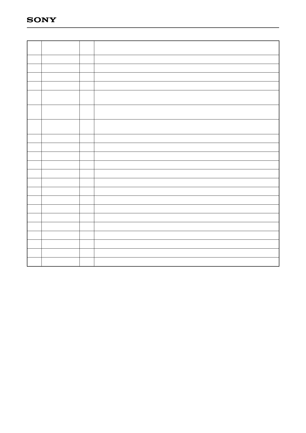
Pin
No.
Symbol
27 TEST
28 TRIG
29 VDD5
30 MCKO
31 SSI
32 SCK
33 SEN
34 VR
35 HR
36 VSS5
37 VM
38 V1
39 V4
40 V2A
41 VH
42 V2B
43 V2C
44 V3A
45 VL
46 V3B
47 V3C
48 SUB
I/O
Description
I IC test pin. normally fixed to GND.
With pull-down resistor
I Trigger mode. Normally fix to power supply.
— 3.3V power supply. (Power supply for common logic block)
O System clock output for signal processing IC.
I
Serial interface data input for internal mode settings.
Schmitt trigger input/protective diode on power supply side.
I
Serial interface data input for internal mode settings.
Schmitt trigger input/protective diode on power supply side.
I
Serial interface data input for internal mode settings.
Schmitt trigger input/protective diode on power supply side.
I/O Vertical sync signal input/output.
I/O Horizontal sync signal input/output.
— GND
I GND (GND for vertical driver)
O CCD vertical register clock output.
O CCD vertical register clock output.
O CCD vertical register clock output.
— 15.0V power supply. (Power supply for vertical driver)
O CCD vertical register clock output.
O CCD vertical register clock output.
O CCD vertical register clock output.
— –7.5V power supply. (Power supply for vertical driver)
O CCD vertical register clock output.
O CCD vertical register clock output.
O CCD electronic shutter pulse output.
–4–
Share Link: 