CXK5T8257BM-10LLX View Datasheet(PDF) - Sony Semiconductor
Part Name
Description
Manufacturer
CXK5T8257BM-10LLX Datasheet PDF : 10 Pages
| |||
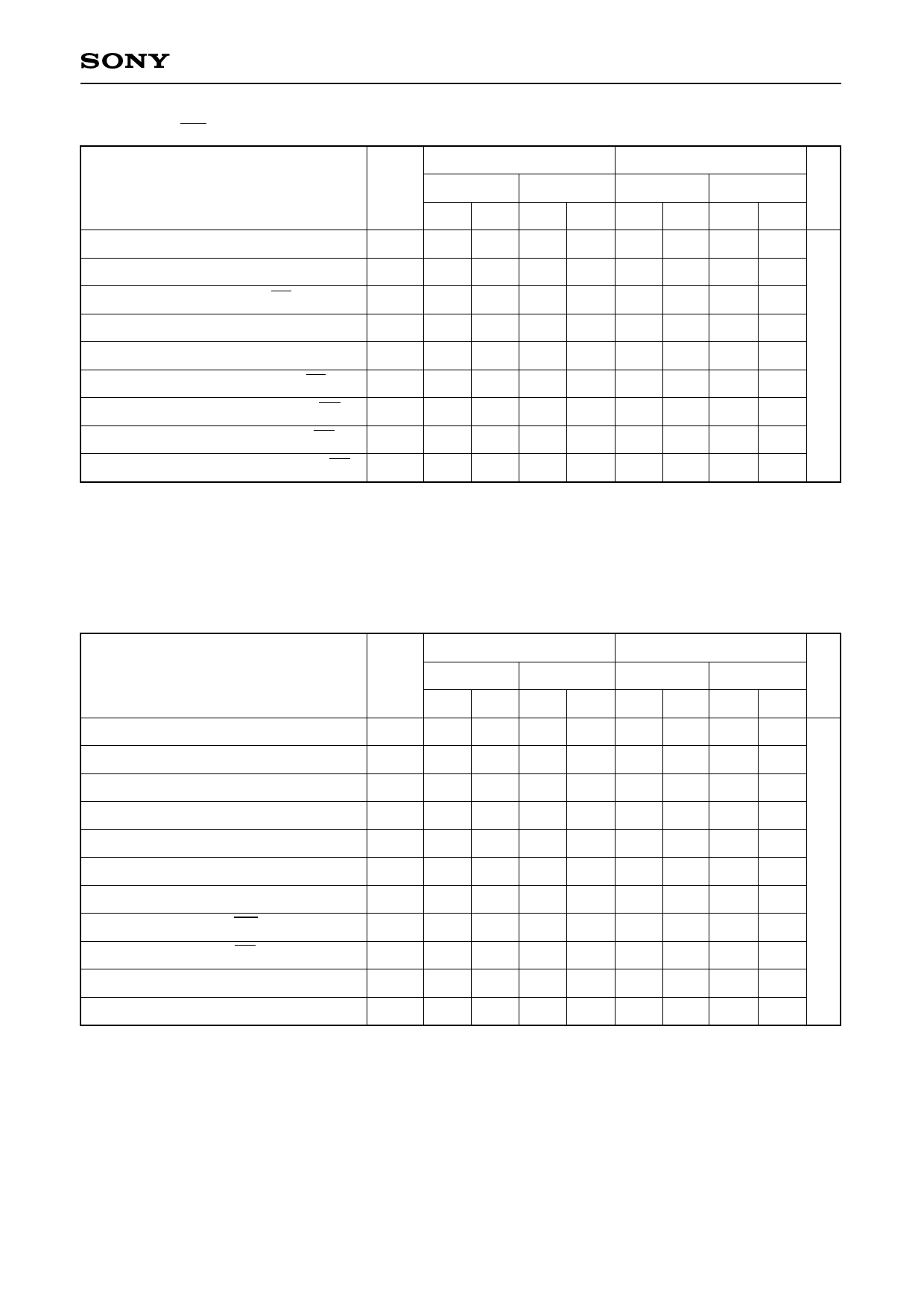
CXK5T8257BTM/BYM/BM
• Read cycle (WE = “H”)
VCC = 2.7 to 3.6V
VCC = 3.3V ± 0.3V
Item
Symbol -10LLX
-12LLX
-10LLX
-12LLX Unit
Min. Max. Min. Max. Min. Max. Min. Max.
Read cycle time
tRC
100 — 120 — 85 — 100 —
Address access time
tAA
— 100 — 120 — 85 — 100
Chip enable access time (CE)
tCO
— 100 — 120 — 85 — 100
Chip enable to output valid
tOE
— 50 — 60 — 50 — 50
Chip hold from address change
tOH
20 — 20 — 20 — 20 — ns
Chip enable to output in low Z (CE)
tLZ
10 — 10 — 10 — 10 —
Output enable to output in low Z (OE) tOLZ 10 — 10 — 10 — 10 —
Chip disable to output in high Z (CE) tHZ∗1 — 35 — 40 — 35 — 35
Output disable to output in high Z (OE) tOHZ∗1 — 35 — 35 — 35 — 35
‚àó1 tHZ and tOHZ are defined as the time required for outputs to turn to high impedance state and are not referred
to as output voltage levels.
• Write cycle
VCC = 2.7 to 3.6V
VCC = 3.3V ± 0.3V
Item
Symbol -10LLX
-12LLX
-10LLX
-12LLX Unit
Min. Max. Min. Max. Min. Max. Min. Max.
Write cycle time
tWC 100 — 120 — 85 — 100 —
Address valid to end of write
tAW
80 — 100 — 80 — 80 —
Chip enable to end of write
tCW
80 — 100 — 80 — 80 —
Data to write time overlap
tDW
35 — 50 — 35 — 35 —
Data hold from write time
tDH
0—0— 0—0—
Write pulse width
tWP
60 — 70 — 60 — 60 — ns
Address setup time
tAS
0—0— 0—0—
Write recovery time (WE)
tWR
0—0— 0—0—
Write recovery time (CE)
tWR1
0—
0—
0—0—
Output active from end of write
Write to output in high Z
tOW
10 — 10 — 10 — 10 —
tWHZ∗2 — 35 — 40 — 35 — 35
‚àó2 tWHZ is defined as the time requied for outputs to turn to high impedance state and is not referred to as
output voltage level.
–5–
Share Link: 