CY62136CV30LL(2006) View Datasheet(PDF) - Cypress Semiconductor
Part Name
Description
Manufacturer
CY62136CV30LL Datasheet PDF : 12 Pages
| |||
CY62136CV30 MoBL®
Maximum Ratings
(Above which the useful life may be impaired. For user guide-
lines, not tested.)
Storage Temperature ................................. –65°C to +150°C
Ambient Temperature with
Power Applied............................................. –55°C to +125°C
Supply Voltage to Ground Potential–0.5V to VCC(max) + 0.5V
DC Voltage Applied to Outputs
in High-Z State[5] ....................................–0.5V to VCC + 0.3V
DC Input Voltage[5] ................................ –0.5V to VCC + 0.3V
Output Current into Outputs (LOW)............................. 20 mA
Static Discharge Voltage.......................................... > 2001V
(per MIL-STD-883, Method 3015)
Latch-up Current.................................................... > 200 mA
Operating Range
Device
CY62136CV30
Ambient
Range Temperature
VCC
Industrial –40°C to +85°C 2.7V to 3.3V
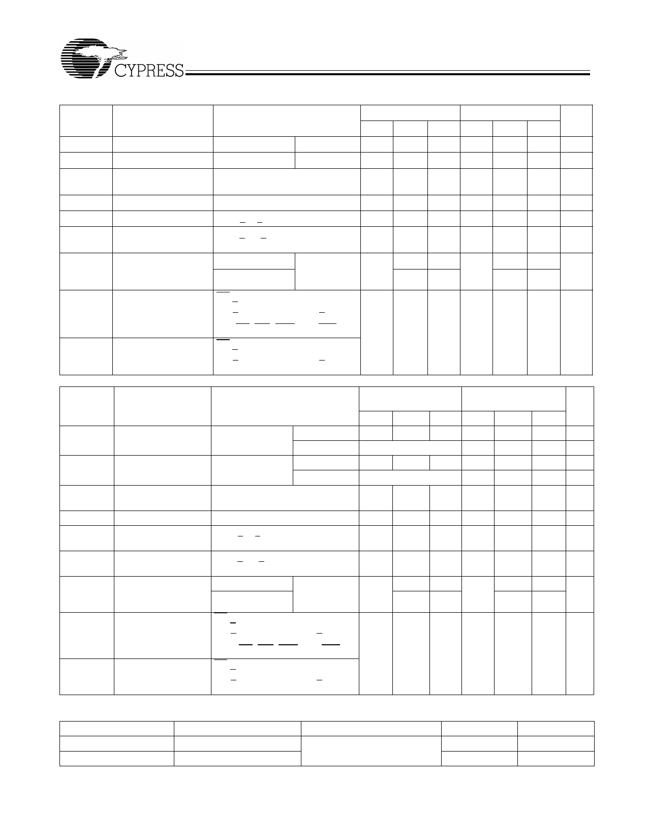
Electrical Characteristics Over the Operating Range
Parameter
Description
Test Conditions
CY62136CV30-55 CY62136CV30-70
Min. Typ.[2] Max. Min. Typ.[2] Max. Unit
VOH
Output HIGH Voltage IOH = –1.0 mA VCC = 2.7V
2.4
VOL
Output LOW Voltage IOL = 2.1 mA
VCC = 2.7V
VIH
Input HIGH Voltage
2.2
2.4
0.4
VCC + 2.2
0.3V
V
0.4 V
VCC + V
0.3V
VIL
Input LOW Voltage
–0.3
IIX
Input Leakage Current GND < VI < VCC
–1
IOZ
Output Leakage
GND < VO < VCC, Output Disabled –1
Current
0.8 –0.3
+1 –1
+1 –1
0.8 V
+1 µA
+1 µA
ICC
VCC Operating Supply f = fMax = 1/tRC VCC = 3.3V
Current
f = 1 MHz
IOUT = 0 mA
CMOS Levels
7
15
1.5 3
5.5 12 mA
1.5 3
ISB1
Automatic CE
CE > VCC – 0.2V
Power-down Current — VIN > VCC – 0.2V or VIN < 0.2V,
CMOS Inputs
f = fMax (Address and Data Only),
f = 0 (OE, WE, BHE, and BLE)
2
10
2
10 µA
ISB2
Automatic CE
CE > VCC – 0.2V
Power-down Current — VIN > VCC – 0.2V or VIN < 0.2V,
CMOS Inputs
f = 0, VCC = 3.3V
2
10
2
10 µA
Capacitance[7]
Parameter
Description
CIN
COUT
Input Capacitance
Output Capacitance
Thermal Resistance[7]
Parameter
Description
ΘJA
Thermal Resistance
(Junction to Ambient)
ΘJC
Thermal Resistance
(Junction to Case)
Test Conditions
TA = 25°C, f = 1 MHz, VCC = VCC(typ.)
Test Conditions
Still Air, soldered on a 3 x 4.5 inch,
2-layer printed circuit board
Max.
6
8
VFBGA
55
16
Unit
pF
pF
Unit
°C/W
°C/W
Notes:
5. VIL(min.) = –2.0V for pulse durations less than 20 ns.
6. Tested initially and after any design or process changes that may affect these parameters.
7. Full Device AC operation requires linear VCC ramp from VDR to VCC(min.) > 100 µs or stable at VCC(min.) > 100 µs.
Document #: 38-05199 Rev. *E
Page 3 of 12
Share Link: 