CY62256V-70RZC View Datasheet(PDF) - Cypress Semiconductor
Part Name
Description
Manufacturer
CY62256V-70RZC Datasheet PDF : 10 Pages
| |||
1CY 622 56 V
fax id: 1069
PRELIMINARY
CY62256V
Features
• 55, 70 ns access time
• CMOS for optimum speed/power
• Wide voltage range: 2.7V−3.6V
• Low active power (70 ns, LL version)
— 108 mW (max.)
• Low standby power (70 ns, LL version)
— 18 µW (max.)
• Easy memory expansion with CE and OE features
• TTL-compatible inputs and outputs
• Automatic power-down when deselected
Functional Description
The CY62256V is a high-performance CMOS static RAM or-
ganized as 32,768 words by 8 bits. Easy memory expansion
is provided by an active LOW chip enable (CE) and active
32K x 8 Static RAM
LOW output enable (OE) and three-state drivers. This device
has an automatic power-down feature, reducing the power
consumption by 98% when deselected. The CY62256V is in
the standard 450-mil-wide (300-mil body width) SOIC, TSOP,
and reverse TSOP packages.
An active LOW write enable signal (WE) controls the writ-
ing/reading operation of the memory. When CE and WE inputs
are both LOW, data on the eight data input/output pins (I/O0
through I/O7) is written into the memory location addressed by
the address present on the address pins (A0 through A14).
Reading the device is accomplished by selecting the device
and enabling the outputs, CE and OE active LOW, while WE
remains inactive or HIGH. Under these conditions, the con-
tents of the location addressed by the information on address
pins is present on the eight data input/output pins.
The input/output pins remain in a high-impedance state unless
the chip is selected, outputs are enabled, and write enable
(WE) is HIGH. A die coat is used to ensure alpha immunity.
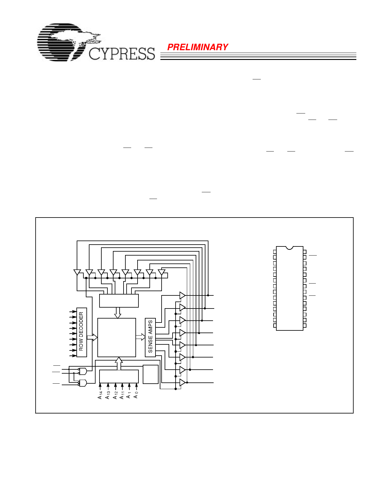
Logic Block Diagram
A10
A9
A8
A7
A6
A5
A4
A3
A2
CE
WE
OE
INPUT BUFFER
512x512
ARRAY
COLUMN
DECODER
POWER
DOWN
Pin Configurations
SOIC
Top View
A5 1
28 VCC
A6 2
A7 3
A8 4
A9 5
A10 6
A11 7
27 WE
26 A4
25 A3
24 A2
23 A1
22 OE
I/O0
A12 8
A13 9
21 A0
20 CE
I/O1
A14 10
I/O0 11
19
18
I/O7
I/O6
I/O1 12
17 I/O5
I/O2
I/O2 13
16 I/O4
GND 14
15 I/O3
I/O3
C62256V–2
I/O4
I/O5
I/O6
I/O7
C62256V–1
Cypress Semiconductor Corporation • 3901 North First Street • San Jose • CA 95134 • 408-943-2600
March 1996 – Revised May 1996
Share Link: 