CY7C1327B-133BGC View Datasheet(PDF) - Cypress Semiconductor
Part Name
Description
Manufacturer
CY7C1327B-133BGC Datasheet PDF : 17 Pages
| |||
CY7C1327B
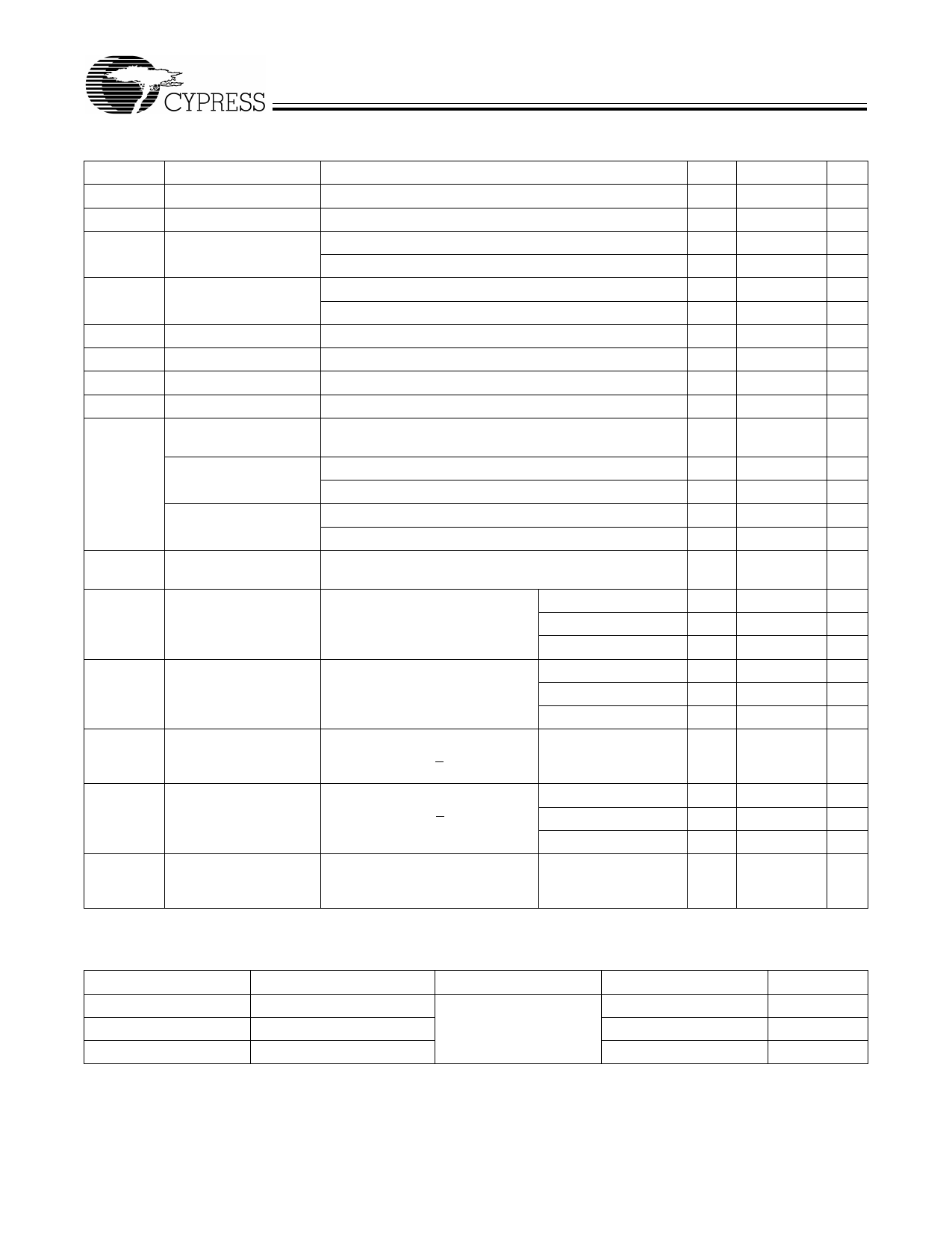
Electrical Characteristics Over the Operating Range
Parameter
Description
Test Conditions
Min.
VDD
VDDQ
VOH
VOL
VIH
VIH
VIL
VIL
IX
Power Supply Voltage
I/O Supply Voltage
Output HIGH Voltage
Output LOW Voltage
Input HIGH Voltage
Input HIGH Voltage
Input LOW Voltage[7]
Input LOW Voltage[7]
Input Load Current
except ZZ and MODE
3.3V −5%/+10%
2.5V −5% to 3.3V +10%
VDDQ = 3.3V, VDD = Min., IOH = –4.0 mA
VDDQ = 2.5V, VDD = Min., IOH = –2.0 mA
VDDQ = 3.3V, VDD = Min., IOL = 8.0 mA
VDDQ = 2.5V, VDD = Min., IOL = 2.0 mA
VDDQ = 3.3V
VDDQ = 2.5V
VDDQ = 3.3V
VDDQ = 2.5V
GND ≤ VI ≤ VDDQ
3.135
2.375
2.4
2.0
2.0
1.7
–0.3
–0.3
−5
Input Current of MODE Input = VSS
−30
Input = VDDQ
Input Current of ZZ
Input = VSS
−5
Input = VDDQ
IOZ
Output Leakage
GND ≤ VI ≤ VDDQ, Output Disabled
−5
Current
IDD
VDD Operating Supply VDD = Max., IOUT = 0 mA,
6-ns cycle, 166 MHz
Current
f = fMAX = 1/tCYC
7.5-ns cycle, 133 MHz
10-ns cycle, 100 MHz
ISB1
Automatic CS
Max. VDD, Device Deselected, 6-ns cycle, 166 MHz
Power-Down
Current—TTL Inputs
VIN ≥ VIH or VIN ≤ VIL
f = fMAX = 1/tCYC
7.5-ns cycle, 133 MHz
10-ns cycle, 100 MHz
ISB2
Automatic CS
Max. VDD, Device Deselected,
Power-Down
VIN ≤ 0.3V or VIN > VDDQ – 0.3V,
Current—CMOS Inputs f = 0
ISB3
Automatic CS
Max. VDD, Device Deselected, or 6-ns cycle, 166 MHz
Power-Down
VIN ≤ 0.3V or VIN > VDDQ – 0.3V
Current—CMOS Inputs f = fMAX = 1/tCYC
7.5-ns cycle, 133 MHz
10-ns cycle, 100 MHz
ISB4
Automatic CS
Max. VDD, Device Deselected,
Power-Down
VIN ≥ VIH or VIN ≤ VIL, f = 0
Current—TTL Inputs
Max.
3.6
3.6
0.4
0.7
VDD + 0.3V
VDD + 0.3V
0.8
0.7
5
5
30
5
420
375
325
150
125
115
10
120
95
85
18
Unit
V
V
V
V
V
V
V
V
V
V
µA
µA
µA
µA
µA
µA
mA
mA
mA
mA
mA
mA
mA
mA
mA
mA
mA
Capacitance[9]
Parameter
Description
Test Conditions
CIN
CCLK
CI/O
Input Capacitance
Clock Input Capacitance
Input/Output Capacitance
TA = 25°C, f = 1 MHz,
VDD = 3.3V,
VDDQ = 3.3V
Note:
9. Tested initially and after any design or process changes that may affect these parameters.
Max.
4
4
4
Unit
pF
pF
pF
Document #: 38-05140 Rev. **
Page 8 of 17
Share Link: 