CY7C1327G(2006) View Datasheet(PDF) - Cypress Semiconductor
Part Name
Description
Manufacturer
CY7C1327G Datasheet PDF : 18 Pages
| |||
CY7C1327G
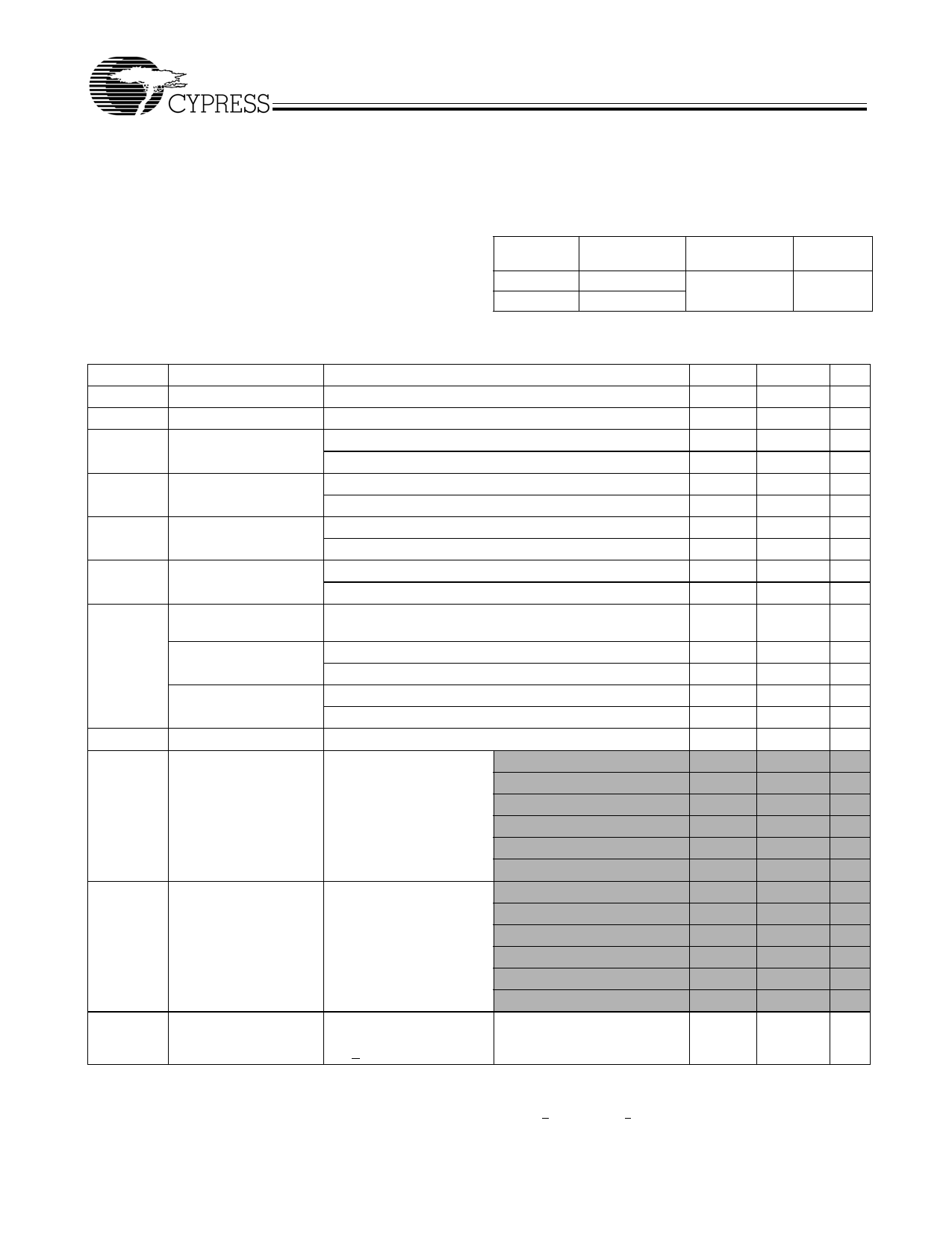
Maximum Ratings
(Above which the useful life may be impaired. For user guide-
lines, not tested.)
Storage Temperature ................................. –65°C to +150°C
Ambient Temperature with
Power Applied............................................. –55°C to +125°C
Supply Voltage on VDD Relative to GND........ –0.5V to +4.6V
Supply Voltage on VDDQ Relative to GND ...... –0.5V to +VDD
DC Voltage Applied to Outputs
in tri-state ............................................ –0.5V to VDDQ + 0.5V
DC Input Voltage ................................... –0.5V to VDD + 0.5V
Current into Outputs (LOW)......................................... 20 mA
Static Discharge Voltage.......................................... > 2001V
(per MIL-STD-883, Method 3015)
Latch-up Current.................................................... > 200 mA
Operating Range
Range
Commercial
Industrial
Ambient
Temperature
VDD
0°C to +70°C 3.3V –5%/+10%
–40°C to +85°C
VDDQ
2.5V –5%
to VDD
Electrical Characteristics Over the Operating Range[7, 8]
Parameter
Description
Test Conditions
VDD
VDDQ
VOH
VOL
VIH
VIL
Power Supply Voltage
I/O Supply Voltage
Output HIGH Voltage
Output LOW Voltage
Input HIGH Voltage[7]
for 3.3V I/O, IOH = –4.0 mA
for 2.5V I/O, IOH = –1.0 mA
for 3.3V I/O, IOL = 8.0 mA
for 2.5V I/O, IOL = 1.0 mA
for 3.3V I/O
for 2.5V I/O
Input LOW Voltage[7] for 3.3V I/O
for 2.5V I/O
IX
Input Leakage Current GND ≤ VI ≤ VDDQ
except ZZ and MODE
Input Current of MODE Input = VSS
Input = VDD
Input Current of ZZ Input = VSS
Input = VDD
IOZ
Output Leakage
GND ≤ VI ≤ VDDQ, Output Disabled
Current
IDD
VDD Operating Supply VDD = Max., IOUT = 0 mA, 4-ns cycle, 250 MHz
Current
f = fMAX = 1/tCYC
5-ns cycle, 200 MHz
6-ns cycle, 166 MHz
7.5-ns cycle, 133 MHz
ISB1
Automatic CE
VDD = Max, Device
4-ns cycle, 250 MHz
Power-down
Current—TTL Inputs
Deselected, VIN ≥ VIH or
VIN ≤ VIL
5-ns cycle, 200 MHz
f = fMAX = 1/tCYC
6-ns cycle, 166 MHz
7.5-ns cycle, 133 MHz
ISB2
Automatic CE
VDD = Max, Device
All speeds
Power-down
Deselected, VIN ≤ 0.3V or
Current—CMOS Inputs VIN > VDDQ – 0.3V, f = 0
Min.
3.135
2.375
2.4
2.0
2.0
1.7
–0.3
–0.3
–5
–30
–5
–5
Max.
Unit
3.6
V
VDD
V
V
V
0.4
V
0.4
V
VDD + 0.3V V
VDD + 0.3V V
0.8
V
0.7
V
5
µA
µA
5
µA
µA
30
µA
5
µA
325
mA
265
mA
240
mA
225
mA
120
mA
110
mA
100
mA
90
mA
40
mA
Notes:
7. Overshoot: VIH(AC) < VDD +1.5V (Pulse width less than tCYC/2), undershoot: VIL(AC) > –2V (Pulse width less than tCYC/2).
8. TPower-up: Assumes a linear ramp from 0V to VDD(min.) within 200 ms. During this time VIH < VDD and VDDQ < VDD.
Document #: 38-05519 Rev. *F
Page 8 of 18
Share Link: 